Boundary scan pioneers go deep
Boundary scan emerged in the 1980s as a way to measure continuity along circuit-board traces and into the I/O pins of devices soldered to the PCBs—all without external probing. Initial work by the Joint Test Action Group (JTAG) led to the IEEE creating the 1149.1 boundary scan standard in 1990. Boundary scan still serves its initial purposes, but pioneers of the technology have moved far beyond the initial PCB trace and chip I/O troubleshooting to probe deep within chips to reach embedded instruments—enabled in part by the new IEEE P1687 Internal JTAG (IJTAG) standard. That standard allows engineers to debug and isolate issues in either a complex SoC or on the circuit board where the chip has been deployed.
ASSET InterTech and Mentor Graphics have teamed up to leverage IJTAG to help isolate problems to the board or chip level. GOEPEL electronic recently announced initiatives related to its technology for processor emulation. And Keysight Technologies has teamed up with Solution Sources Programming (SSP) to provide enhanced boundary scan capabilities to augment traditional in-circuit test (ICT) for printed-circuit board assemblies (PCBAs) that provide limited access for physical test probes.
At the International Test Conference last fall, ASSET InterTech took the opportunity to highlight seamless interoperability between ASSET InterTech’s ScanWorks platform and Mentor Graphics’ Tessent products for IJTAG embedded instrumentation. Tim Caffee, ASSET’s vice president of design validation and test, said at the time that the IJTAG standard defines access to portable and reusable embedded instruments. The standard, he said, has three components: a flexible serial instrument access architecture (called the network), a network description language (called Instrument Connectivity Language, or ICL), and an instrument vector language (called the Procedure Description Language, or PDL). The architecture comprises a controller, access network, and embedded instruments. IJTAG applications include silicon validation and debug at the board level, at-speed flash programming of NOR and NAND devices via SPI or I2C, SerDes validation (including PCIe, SATA, PEG, and USB), and memory validation (including DDR3 and DDR4).
Caffee described an IJTAG flow and two-way validation process that ends finger-pointing as to whether a problem lies at the chip or board level. EDA companies such as Cadence, Mentor, and Synopsis handle IJTAG insertion, simulation, ATPG, and emulation in FPGAs; ASSET supports board validation, test, and debug; and all parties contribute to the middle ground of silicon test on ATE and silicon validation.
Caffee and Stephen Pateras, product marketing director at Mentor Graphics, have recently written, “The newly approved IEEE 1687 standard … is changing the way tools companies like ours think about interoperability. For example, IJTAG interoperability is tremendously valuable at both the chip and circuit-board levels because of the re-use of embedded instrumentation intellectual property (IP). Moreover, when chip- and board-level IJTAG tools feature two-way or back-and-forth interoperability, all of the tools in the flow become more powerful than they could be on their own. Call it the power of synergy.”1
ASSET and Mentor are collaborating on several educational programs to jump-start the adoption of IJTAG, including a series of workshops in major technology hubs in the United States, Asia, and Europe.
Targeting controllers and FPGAs
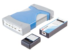
At the APEX Expo in February, JTAG Technologies highlighted its CoreCommander (Figure 1) and JTAG Translator tools for FPGAs, which combine to provide direct access to memory and peripheral controllers in
Courtesy JTAG Technologies
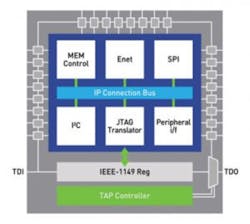
FPGAs for testing, debugging, and in-system programming. JTAG Translator is an IP module that provides a JTAG interface to the internal IP connection bus of an FPGA to which peripherals and peripheral controllers are connected.
JTAG Translator is operated through a dedicated CoreCommander that can be used with JTAGLive and ProVision tools as well as with all of the company’s production packages. CoreCommander provides high-level functions to write data to and read data from memory and I/O addresses without software programming, with CoreCommander functions applied via the JTAG interface. The JTAG Translator IP module can be loaded in the FPGA for test configurations only, or it can be included as standard in functional designs.
With JTAG Translator, the IP blocks that already are used in a design can be reused for test or in-system programming purposes. Examples of existing IP blocks are interface controllers for SDR, DDR, Ethernet MAC, USB, UART, I2C, and CAN. These IP blocks are available from different IP suppliers like Altera, Xilinx, and OpenCores.
Processor emulation
GOEPEL electronic recently announced two initiatives related to its VarioTAP technology for universal processor emulation. As the company describes it, VarioTAP turns a processor into a design-integrated test and programming instrument. The user can select the processor model and then test and validate the connected hardware units as well as in-system programming of flash memories. The use of VarioTAP does not require probes for contacting the UUT. The technology is part of
GOEPEL’s Embedded System Access technology, complementing other nonintrusive test methods.
For example, GOEPEL recently announced the development of model libraries for testing and programming of Intel Bay Trail processors, which are part of the Intel Atom family. The VarioTAP models allow flexible execution of processor emulation tests using the native debug port. The processor can serve as an instrument for hardware design validation of prototypes as well as programming of flash devices. Bay Trail includes a series of multicore SoC devices based on the Silvermont Intel architecture. Manufactured in a 22-nm process, the chips offer optimized performance with low energy consumption. Bay Trail processors address mobile applications such as tablets and notebooks as well as hybrid and embedded devices. Versions offer up to four processor cores and clock speeds up to 2 GHz.
The processors are integrated in μFCBGA (micro flip chip ball grid array) packages with several hundred pins that are mounted directly on the board, not allowing direct contact with external instruments (Figure 2). VarioTAP supports programming and design validation even after mounting.
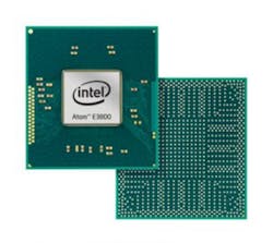
Courtesy of GOEPEL electronic
And at embedded world 2015 in February in Nuremberg, GOEPEL announced the availability of the VarioTAP software option for the Infineon TriCore AURIX processors. Support for Infineon architectures will be expanded through the new models. AURIX processors belong to the latest TriCore generation and are mainly used in automotive electronic control units.
GOEPEL also recently announced a strategic cooperative agreement with KOZIO with the aim of developing new embedded tools. A particular focus will be on real-time solutions for validation and production test of complex microprocessor controlled designs, which is relevant for the Internet of Things. As the first result of the cooperation, GOEPEL will demonstrate a beta version of a JTAG-controlled integration of KOZIO’s VTOS DDR tools into GOEPEL’s SYSTEM CASCON software platform. The tool has been developed by KOZIO for embedded performance test of DDR memories.
Boundary scan analyzer
Keysight Technologies announced in March that SSP has achieved significant boundary scan test capabilities using the Keysight x1149 boundary scan analyzer in a standalone configuration or integrated with the Keysight i3070 ICT system.
SSP has used the Keysight x1149-based solution on 11 key projects, the companies report, with applications ranging from low to no-access boards all the way up to the most complex 50,000-joint network circuit boards of more than 9,250 nets.
“Today’s technology is minimizing physical accessibility for traditional ICT,” said Eric Harris, SSP’s cofounder and senior engineering manager, in a press release. “Many people believe that when a board falls below 50% access, they should look for alternatives to ICT. By using modern platform and fixturing technology, we are able to consistently show customers how to recapture lost coverage and ultimately give their contract manufacturing partners the diagnostics needed to ensure there are no manufacturing defects getting through their line. It’s just about pairing up the right tools for the job.”
Densely populated networking circuit boards face multiple issues when using traditional ICT techniques. Challenges range from not having enough physical space for optimal test points to high-speed signal transmission and signal integrity concerns and, in some cases, multiple boundary scan chains on one board. The small form-factor of the Keysight benchtop x1149 (Figure 3) fits on an in-circuit tester to enable a complimentary suite of test capabilities with its ease of use and manufacturing readiness. The x1149 also produced faster test times with its Autobank diagnosis capabilities.
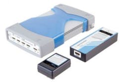
Courtesy of Keysight Technologies
“We have done some amazing things using the x1149 combined with the 3070. One customer had more than 90 DDRs on its assembly—an area that we traditionally wouldn’t test due to elongated test times. Our team was able to not only test these DDRs at ICT, but also did it in less than 60 seconds. Traditional methods would take more than five minutes,” added Harris.
In addition, boards with limited or no test access, such as tablets or small phones, also can benefit from such tools. Keysight’s unique Cover-Extend technology and its Silicon Nails boundary scan capabilities help expand coverage in crucial areas of the boards.
“We have had boards with less than 25% access,” said Dan Orlando, SSP’s president and cofounder. “By combining ICT with the x1149, we were able to bring back coverage to the 90% range. We’ve been able to deliver significant improvements in test coverage by leveraging our expertise and tools, such as the x1149 to expand our capability in all markets—including tablets, SSD drives, and server and networking PCBAs.”
He added, “As board designs increase in complexity, SSP continues to innovate and enable customers to use their extensive boundary scan experience with Keysight’s x1149 platform. The x1149 is truly built for manufacturing test. The graphical user interface is intuitive and easy to use, allowing our team to develop and debug tests quickly so that board tests can be implemented rapidly in production for our customers. As engineering teams continue to come out with new designs challenging traditional conventions of manufacturing test, we pride ourselves in creating a manufacturing plan that not only helps their contract manufacturers, but also ultimately helps protect their brand equity by capturing faults early in the line.”
Keysight’s product development team continues to extend the application capabilities of the x1149 and collaborate closely with electronics leaders to enhance product quality through innovative boundary scan solutions.
“The combination of SSP’s expertise in developing test applications, together with the extensive boundary scan test capabilities of the x1149, have resulted in improved test coverage,” said NK Chari, director of marketing and support from Keysight’s Measurement Systems Division. “In addition, we have seen an improvement in test time on today’s highly sophisticated PCBAs, ranging from networking and server cards to consumer electronic PCBAs found in tablets and smartphones. We are application-ready and look forward to helping our customers win with better boundary scan test.”
Reference
1. Pateras, S., and Caffee, T., “IJTAG interoperability brings value to chip and board engineers,” EE-Evaluation Engineering, Jan. 16, 2015.
FOR MORE INFORMATION
About the Author
Comment About the Article
To join the conversation, and become an exclusive member of Electronic Design, create an account today!

Leaders relevant to this article: