In 2015, there’s not much question about audio storage, transmission, or streaming: it’s digital. Apart from rare sightings of vinyl or open-reel tape in boutique sales or creative enclaves, audio is digital. Done right, digital audio is flexible, robust, and of very high quality. Pulse code modulation (PCM) recording, lossless surround formats, and even lossy compression (at least at high data rates) provide the soundtrack for our lives.
But, of course, sound in air is not digital. The pressure waves created by a human voice or a musical instrument are recorded after exciting a transducer of some sort, and the transducer responds with an electrical voltage that is an analog of the pressure wave. Likewise, at the end of the chain, the digitized audio signal must eventually move air, using a voltage that is the analog of the original sound wave to drive a transducer that creates a pressure wave.
Near the beginning of a digital chain, then, we must use an analog-to-digital converter (ADC) to transform the analog electrical signal to a digital representation of that signal. Near the end of the chain, we must use a digital-to-analog converter (DAC) to transform the digital audio signal back into an analog electrical signal. Along with the transducers, these two links in the chain (the ADC and the DAC) are key in determining the overall quality of the sound presented to the listener.
Testing audio converters
The conventional measurements used in audio test also can be used to evaluate ADCs and DACs. These measurements include frequency response, signal-to-noise ratio (SNR), interchannel phase, crosstalk, distortion, group delay, and polarity. But conversion between the continuous and sampled domains brings a number of new mechanisms for nonlinearity, particularly for low-level signals.
Of course, ADCs and DACs are used in a great number of nonaudio applications, often operating at much higher sampling rates than audio converters. Very good oscilloscopes might have bandwidths of 33 GHz and sampling rates up to 100 GS/s, with prices comparable to a Lamborghini. Although audio converters don’t sample at anywhere near that rate, they are required to cover a much larger dynamic range, with high-performance ADCs digitizing at 24 bits and having SNRs greater than 120 dB. Even a high-end oscilloscope typically uses only an 8-bit digitizer. 24-bit conversion pushes the measurement of noise and other small-signal performance characteristics to the bleeding edge; consequently, measurements of such converters require an analyzer of extraordinary analog performance.
Test setups
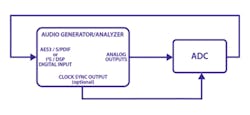
The typical test setups are straightforward. For ADC testing (Figure 1), the analyzer must provide extremely pure stimulus signals at the drive levels appropriate for the converter input. For converter ICs, the analyzer must have a digital input in a format and protocol to match the IC output, such as I2S, DSP, or a custom format. For a commercial converter device, the digital format typically is an AES3-S/PDIF-compatible stream. For devices that can sync to an external clock, the analyzer should provide a clock sync output.
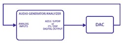
For DAC testing (Figure 2), the analyzer must have a digital output in the appropriate format and analog inputs of very high performance.
The graphs in this article were created by testing commercial converters, using the AES3 digital transport. The analyzer is the Audio Precision APx555.
As mentioned previously, ADCs and DACs exhibit behaviors unique to converters. The Audio Engineering Society has recommended methods to measure many converter behaviors in the AES17 standard. The following examples examine and compare a number of characteristic converter issues.
Idle tones
Common audio converter architectures, such as delta-sigma devices, are prone to have an idling behavior that produces low-level tones. These “idle tones” can be modulated in frequency by the applied signal and by DC offset, which means they are difficult to identify if a signal is present. An FFT of the idle channel test output can be used to identify these tones.
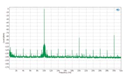
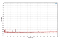
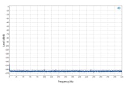
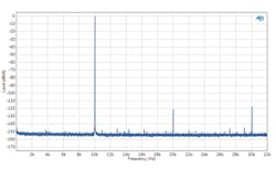
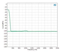
The DAC in Figure 3 shows a number of idle tones, some with levels as high as -130 dB. The idle tones (and the noise floor) in Figure 4 are much lower.
Signal-to-noise ratio (Dynamic range)
For analog audio devices, an SNR measurement involves finding the device maximum output and the bandwidth-limited rms noise floor and reporting the difference between the two in decibels.
With audio converters, the maximum level usually is defined as that level where the peaks of a sine wave just touch the maximum and minimum sample values. This is called “full scale” (1 FS), which can be expressed logarithmically as 0 dBFS. The rms noise floor is a little tricky to measure because of low-level idle tones and, in some converters, muting that is applied when the signal input is zero. AES17 recommends that a -60 dB tone be applied to defeat any muting and to allow the converter to operate linearly. The distortion products of this tone are so low they fall below the noise floor, and the tone itself is notched out during the noise measurement. IEC 61606 recommends a similar method but calls the measurement dynamic range.
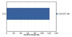
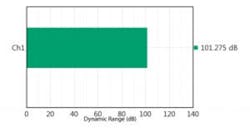
Figures 5 and 6 show a comparison of the signal-to-noise measurements of two 24-bit DACs operating at 96 kS/s using this method. As can be seen, some converter designs are much more effective than others.
Jitter
For ADCs, clock jitter can occur within the converter, and synchronization jitter can be contributed through an external clock sync input. For DACs receiving a signal with an embedded clock (such as AES3 or S/PDIF), interface jitter on the incoming signal must be attenuated.
Sinusoidal jitter primarily affects the audio signal by creating modulation sidebands, frequencies above and below the original audio signal. More complex or broadband jitter will raise the converter noise floor. A common measurement that reveals jitter susceptibility is to use a high-frequency sinusoidal stimulus and examine an FFT of the converter output for jitter sidebands, which are symmetrical around the stimulus tone. In Figures 7 and 8, DAC C shows strong sidebands while DAC B shows none. Note that the strong tones at 20 kHz and 30 kHz are products of harmonic distortion and not jitter sidebands.

Jitter tolerance template
AES3 describes a jitter tolerance test where the capability of a receiver to tolerate defined levels of interface jitter on its input is examined. A digital audio signal is applied to the input. The signal is jittered with sinusoidal jitter, swept from 100 Hz to 100 kHz. As the jitter is swept, its level is varied according to the AES3 jitter tolerance template. Jitter is set at a high level up to 200 Hz, then reduced to a lower level by 8 kHz, where it is maintained until the end of the sweep.
An interface data receiver should correctly decode an incoming data stream with any sinusoidal jitter defined by the jitter tolerance template of Figure 9. The template requires a jitter tolerance of 0.25 unit interval (UI) peak-to-peak at high frequencies, increasing with the inverse of frequency below 8 kHz to level off at 10 UI peak-to-peak below 200 Hz.
In this case, jitter is set to about 9.775 UI at the lower jitter frequencies and drops to about 0.25 UI at the higher frequencies. The blue trace is the THD+N ratio (distortion products of the 3-kHz audio tone), which remains constant across the jitter sweep, indicating good jitter tolerance in this DUT. As the jitter level rises, poor tolerance will cause a receiver to decode the signal incorrectly and then fail to decode the signal, occasionally muting or sometimes losing lock altogether.
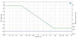
Figure 10 shows the response of the anti-alias filter in ADC C. A tone at the input of the ADC is swept across the out-of-band (OOB) range of interest (in this case, from 40 kHz to 200 kHz), and the level of the signal reflected into the passband is plotted against the stimulus frequency. A second trace shows the converter noise floor as a reference.
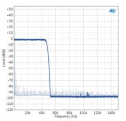
For Figure 11, spectrally flat random noise is presented to the DAC input. The analog output is plotted (with many averages) to show the response of the DAC’s anti-image filter. In this case, a second trace showing a 1-kHz tone and the DAC noise floor is plotted, scaled so that the sine peak corresponds to the noise peak.
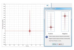
Polarity
Audio circuits (including converters) often use differential (balanced) architectures. This opens the door for polarity faults. An impulse response stimulus provides a clear observation of normal or reversed polarity (Figure 12).
Summary
Tests for the high-level nonlinear behavior of an ADC are similar to those for nonlinearities in analog electronics, using standardized tests for harmonic distortion and intermodulation distortion. But audio converters bring new mechanisms for nonlinearity, particularly for low-level signals. AES171 and Audio Precision’s Technote 1242 describe effective testing methods for audio converter measurements.
References
1. AES17-1998 (r2009), “AES standard method for digital audio engineering—Measurement of digital audio equipment,” Revision of AES17-1991.
2. Peterson, S., Measuring A-to-D and D-to-A Converters with APx555, Audio Precision, Technote 124, 2015.
For further reading
- AES3-2009 (r2014), “AES standard for digital audio engineering—
Serial transmission format for two-channel linearly represented digital audio data.” - Dunn, J., Measurement Techniques for Digital Audio, Audio Precision, Application Note #5, 2004. (Although written in 2001 and illustrated with examples made on older measurement systems, App Note #5 nonetheless examines in relevant ways jitter theory and the digital interface transport stream and looks in detail at the practice of measurement in ADCs and DACs.)
About the author
David Mathew is technical publications manager and a senior technical writer at Audio Precision. He has worked as both a mixing engineer and as a technical engineer in the recording and filmmaking industries and was awarded an Emmy for his sound work in 1988. [email protected]
Glossary
AES: Audio Engineering Society, with headquarters in New York City
AES3, S/PDIF: In the consumer and professional audio field, digital audio typically is carried from point to point as a biphase coded signal, commonly referred to as AES3, AES/EBU, or S/PDIF. There are electrical and bit-stream protocol differences among the variations of biphase coded digital audio, but the various signals are largely compatible. Variations are defined in the standards AES3, IEC 60958, and SMPTE276M.
Anti-alias filter: In sampled systems, the bandwidth of the input has to be limited to the folding frequency to avoid aliasing. Modern audio ADCs normally have this anti-alias filter implemented with a combination of a sharp-cutoff finite impulse response (FIR) digital filter and a simple low-order analog filter. The digital filter operates on a version of the signal after conversion at an oversampled rate, and the analog filter is required to attenuate signals that are close to the oversampling frequency. This analog filter can have a relaxed response since the oversampling frequency often is many octaves above the passband.
Anti-image filter (reconstruction filter): Digital audio signals can only represent a selected bandwidth. When constructing an analog signal from a digital audio data stream, a direct conversion of sample data values to analog voltages will produce images of the audio band spectrum at multiples of the sampling frequency. Normally, these images are removed by an anti-imaging filter. This filter has a stopband that starts at half of the sampling frequency—the folding frequency. Modern audio DACs usually have this anti-imaging filter implemented with a combination of two filters: a sharp cutoff digital finite impulse response (FIR) filter, followed by a relatively simple low-order analog filter. The digital filter is operating on an oversampled version of the input signal, and the analog filter is required to attenuate signals that are close to the oversampling frequency.
PCM: Pulse code modulation, a form of data transmission in which amplitude samples of an analog signal are represented by digital numbers.
UI: The unit interval is a measure of time that scales with the interface data rate and often a convenient term for interface jitter discussions. The UI is defined as the shortest nominal time interval in the coding scheme. For an AES3 signal, there are 32 bits per subframe and 64 bits per frame, giving a nominal 128 pulses per frame in the channel after biphase mark encoding is applied. So, in our case of a sampling rate of 96 kHz,
1 UI = 1/(128 x 96000) = 81.4 ns
The UI is used for several of the jitter specifications in AES3.
Sidebar
Interpretation of noise in FFT power spectra
In audio systems, noise figures generally are measured and reported something like this:
-103 dB rms noise, 20 Hz to 20 kHz BW, A-weighted
The noise signal is measured with an rms detector across a specified bandwidth. The 0-dB reference for the noise measurement might be the nominal operating level of a device but more typically is the maximum operating level, which produces a more impressive number. Similarly, weighting filters usually produce better noise figures and so often are used in marketing specifications. A weighting filter attempts to approximate the response that we humans perceive.
So let’s measure the noise of DAC B using these methods. We’ll make an rms measurement first across the full signal bandwidth, then across a limited bandwidth, then with an added weighting filter.
- -120.3 dB rms noise, DC to 48 kHz
- -123.9 dB rms noise, 20 Hz to 20 kHz
- -126.2 dB rms noise, 20 Hz to 20 kHz, A-weighted
But if you look at the FFT spectrum shown in Figure 4, the average noise floor appears to be about -163 dB or so. That’s a big difference. What’s up?
Conventionally, an audio FFT amplitude spectrum is displayed by scaling the vertical axis so that a bin peak indicates a value that corresponds to the amplitude of any discrete frequency components within the bin. This calibration is not appropriate for measuring broadband signals, such as noise power, without applying a conversion factor that depends on the bin width and on the FFT window used.
In this case, each bin is 0.375 Hz wide (sample rate of 96 kS/s divided by an FFT length of 256k points).
The window spreads the energy from the signal component at any discrete frequency, and the Y-axis calibration takes this windowing into account. For the AP Equiripple window used here, the calibration compensates for the power being spread over a bandwidth of 2.63 bins.
This can be converted to the power in a 1-Hz bandwidth, or the power density, by adding a scaling factor in decibels that can be calculated as follows:
scaling factor = 10log(1/window scaling × bin width)
= 10log(1/2.63 × 0.375)
= 4.2 dB
To estimate the noise from a device based on an FFT spectrum, you can integrate the power density over the frequency range of interest. For an approximately flat total noise (where the noise power density is roughly constant), it is possible to estimate the sum of the power in each bin within reasonable accuracy by estimating the average noise power density and multiplying by the bandwidth.
Figure 4, for example, has a noise floor that is approximately in line with about -163 dB on the Y axis. The noise power density is the apparent noise floor minus the window conversion factor or
-163 dB – 4.2 dB = -167.2 dB per Hz
The integration to figure the total noise over a given bandwidth is simple if the noise is spectrally flat. Multiply the noise power density by the bandwidth, which in this case is 20 kHz. For dB power (dB = 10logX), this is the same as adding 43 dB (= 10log(20000)), as follows:
-167.2 + 43 dB = -124.2 dB
This calculation provides a result only ½ dB different from the 20-Hz to 20-kHz unweighted measurement cited above.
About the Author

Comment About the Article
To join the conversation, and become an exclusive member of Electronic Design, create an account today!

Leaders relevant to this article: