Tomorrow’s chip interconnects call for a new reliability test method

Undaunted by the skyrocketing costs of new semiconductor fabs and the formidable hurdles facing the industry with each new technology node, leading IC manufacturers are continuing to strive for shrinking geometries. Much recent attention has been paid to transistor advances such as fin-shaped field-effect transistors, but significant work is necessary in parallel to create ever smaller back end-of-line (BEOL) interconnects—the conductors which connect those transistors. With tens of thousands of meters of interconnect and billions of connections in today’s advanced microprocessors, conductor reliability is a vital element of IC longevity.
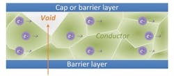
Figure 1. Electromigration in a copper line
The primary long-term wearout mechanism in conductors is electromigration (EM), a phenomenon whereby the stress of current flowing through the metal creates voids or gaps (Figure 1). These voids grow over time and ultimately result in IC failure. For decades, the mainstream method for evaluating and predicting this phenomenon has been constant current EM (CIEM). However, researchers now see serious problems with broadly applying the venerable CIEM test approach to the next generations of interconnects. Upcoming material and aspect ratio changes in copper lines and vias and the barrier layers protecting those conductors may herald a sea-change in reliability test methods. A new test method called constant voltage EM (CVEM) offers a solution.
Collect high-quality data
EM test results help establish rules and guidelines for IC designers to properly balance the competing goals of circuit speed and power vs. reliability and longevity. It’s increasingly important that the data feeding these design rules is accurate as EM lifetimes have been observed to drop by approximately half with each new technology node. IC designers today have very little safety margin, and a crude approximation will not be sufficient for tomorrow’s technologies.
EM testing subjects sacrificial structures to a variety of elevated electrical and thermal stress conditions to accelerate their degradation. Failure times (usually on the order of weeks) are extrapolated via mathematical models to predict lifetime τ at normal IC usage conditions, per Black’s Equation:
To yield useful design rules, high-quality data must be collected for the reliability models. Good test methods will ensure that accelerated failures are the same as those that occur under normal IC use conditions, failure times are accurately determined and easily extracted from the test data, and stress conditions are accurately and consistently applied to all test samples. CIEM will be hard pressed to deliver on these requirements for advanced interconnect technologies.
The “right” failures
Different methods yield different behavior, and the first challenge for EM tests is ensuring the failures under accelerated test are identical to those experienced by ICs in the field. The CIEM method has worked fine for all previous generations of copper BEOL interconnects, but advanced technology nodes present new challenges, especially due to changes in the barrier layer. As copper lines become narrower with each new node, they have less cross-sectional area, increased line edge roughness (LER), and smaller grains—all of which lead to more surface scattering and higher line resistance. In turn, this impacts circuit performance with transmission delays and heat. To combat these negative effects, interconnect designers maximize the conductor cross-sectional area by developing thinner barriers (the material that wraps the copper lines to prevent interaction with the ultralow-k dielectric). More room in the trenches for the copper conductor provides additional area, but the thinner barriers generate new issues.
Past generations of barrier materials such as TaNTa have served as “relief valves” for EM—when large voids occur in the copper, the barriers act as shunt paths and share some of the electron flow around the void. However, TaNTa (applied to trench walls via physical vapor deposition) cannot be evenly and thinly applied into future trenches which have a very high aspect ratio (that is, lines are very narrow compared to their depth). Proposed solutions such as manganese-based self-forming barriers promise to provide very thin and uniform barrier protection, but unfortunately they also are essentially nonconductive and therefore ineffective for shunting current.
How does this impact the CIEM test? Picture a copper line where a void begins to grow due to EM. With ultrathin barriers, the current has no shunt path and must flow entirely through the small amount of remaining conductor around the void. Ohm’s Law indicates that if we are forcing a constant current I (using CIEM) through this high-resistance R pinch point, we will see a high voltage drop V in that region. Most traditional EM test systems have a voltage compliance of several volts (well above the operating voltage for advanced CMOS), which means that localized high voltage and heat conditions occur during CIEM test that would never occur in a voltage-driven line most common in CMOS logic. CIEM may remain appropriate for the current-driven lines in an IC, but for voltage-driven circuitry, it clearly violates the first test design requirement of mimicking only true field-failure behavior.
Conversely, CVEM is similar to the operation of voltage-driven lines, and Ohm’s Law shows that the current through the pinch point actually will drop as the resistance increases due to voids. Overstress does not occur, and failures generated this way match real-world results, qualifying CVEM as the more appropriate test method.
Clean failure detection
The CIEM overstress condition yields some fascinating results that complicate the task of establishing a fail time for structures under test (Figure 2). The familiar shape of plot 2a will give way in future interconnect generations with nonconductive barriers to either plot 2b or plot 2c, depending on the test method.
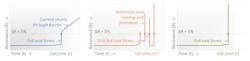
Figure 2b. Next-generation copper interconnect with nonconductive barrier (CIEM stress)
Figure 2c. Next-generation copper interconnect with nonconductive barrier (CVEM stress)
EM failure times normally correspond to a change in resistance of the test structure, such as 5%, which is enough to impact the performance of a larger circuit. The resistance change indicates a reduction in cross-sectional area—that is, the presence of a void in the path. It traditionally has been clearly determined as in plot 2a, but an examination of plot 2b does not reveal an obvious fail time. The resistance crosses the failure threshold but then often recovers, possibly repeating this cycle numerous times before the line finally becomes an open circuit. It is conjectured that this self-healing behavior is due to upstream copper atoms, mobilized by the high local stresses, which vacate their original positions to refill the primary void. These multiple failure events all can be considered “false failures” because they are created under unrealistic conditions.
Which of the false-failure events is closest to representing the structure’s true fail time? The most conservative view is to look at the first event, but these failure-recovery cycles can happen very quickly and thus the capability of the measurement equipment comes into play. Many commercial EM test systems measure too slowly to capture these transient effects. Further complicating confirmation of the correct failure mechanism is the fact that this self-healing recovery behavior refills voids before the structures can be removed from test and examined with a scanning electron microscope.
With all these uncertainties, CIEM clearly cannot meet requirements of providing a clear and accurate measurement of fail time for structures with nonconductive barriers. Fortunately, CVEM provides a solution. Notice the very clean failure behavior of the test structures in plot 2c. There is no ambiguity about the structure’s fail time.
The third challenge for successful EM testing lies in providing an accurate stress bias—the method matters as much as good test equipment. Reliability testing is a statistical exercise; decisions are made on results from a set of samples rather than a single structure so it is important all these samples are stressed identically. In the case of applying CIEM to highly scaled interconnects, the structures themselves can corrupt the bias conditions. This is because the EM wearout phenomenon is a function not of current I, but rather current density J (where J = I/A, and A is the cross-sectional area of the structure).
With very small lines, natural variation from structure to structure can be significant. Factors such as LER, which could be ignored for previous generations’ larger structures, now are becoming proportionally significant error sources. This is a well-known challenge for continued scaling, and the International Technology Roadmap for Semiconductors lists the roughness of lines and barriers among the top five most critical challenges for interconnects in technologies smaller than 16 nm.
For CIEM tests, where the same current stress is applied to all structures in a sample set, variance in A from sample to sample means each of those structures actually will experience a slightly different (and not precisely known) current density. Since structure breakdown is accelerated by current density, this will unpredictably shift each structure’s failure times. This is evidenced by a broader sigma value in the data’s lognormal analysis. This yields a higher level of statistical uncertainty when the accelerated results are extrapolated to normal use conditions.
With CVEM, current flow is a function of the electric field E (E = V/L, where L is the length of the structure). Since line lengths are several orders of magnitude greater than their widths, geometrical variations of L are proportionally insignificant. CVEM’s voltage bias will yield a very consistent E-field across all samples and therefore eliminate the bias corruption that plagues the CIEM method on advanced interconnects.
Conclusion
Shrinking semiconductor geometries with reduced reliability margins demand a highly accurate method for modeling EM effects to produce proper IC design rules. Inaccurate EM results, corrupted by the false-failure phenomena and stress variance which arise when applying the traditional CIEM test method to the next generations of interconnects, could lead to falsely pessimistic EM models that in turn can handcuff designers and limit chip specifications in a highly competitive market. Conversely, the same error sources could yield falsely optimistic EM models, which leave an IC manufacturer vulnerable to costly field failures and a damaged reputation. For voltage-driven lines, CVEM offers a precise solution to avoid these pitfalls and enable IC manufacturers to continue offering aggressive performance specifications without sacrificing quality.
About the Author
Timothy McMullen is the director of product marketing for Cascade Microtech’s lineup of reliability test equipment. Previously, he served as the general manager for Aetrium’s reliability test products division. [email protected]
About the Author
Comment About the Article
To join the conversation, and become an exclusive member of Electronic Design, create an account today!

Leaders relevant to this article: