Design for Test: Impacting accuracy of chipmaker’s quality tests
Near the beginning of every chip design project, the design team will have a debate about the trade-off between cost and quality. One of the most vexed questions tends to be about the value of incorporating dedicated test modes into the circuit design—that is, about adopting a design for test (DFT) approach.
On the one hand, DFT adds design work and increases the die area to accommodate test functionality that is not used in the end application. On the other, DFT can enable more precise and/or more accurate testing of the chip’s characteristics. This enables the manufacturer to improve quality because the performance of each shipped unit can more closely match the device’s specifications as documented in the datasheet.
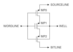
At ams, an automotive-qualified (ISO/TS16949) manufacturer of analog and mixed-signal semiconductors, quality is of paramount importance, and this gives the company a close-up view of the value of DFT—even in the digital parts of mixed-signal products. This article uses the example of an EEPROM IP block to show how DFT enables more accurate characterization of the block and the impact that this has on the quality of devices shipped to automotive customers. Figure 1 shows the architecture of an EEPROM bit cell.
EEPROMs: the determinants of quality
For the user of an EEPROM, a type of nonvolatile memory, quality normally is specified in the following terms:
- the number of write/erase cycles it can support, and
- the length of time it can retain data. A typical requirement is for 10 years’ data retention.
These quality measures are, in turn, determined by three characteristics of an EEPROM die:
- endurance loops (the number of write operations the EEPROM can withstand before it can no longer be programmed),
- the input voltage at which a bit cell can be programmed and erased, and
- the charge held in a bit cell after a write operation.
The bit cell charge is important because, over time, charge leaks from a programmed cell. The initial charge when programmed must be sufficiently high to allow for this leakage while still guaranteeing the full 10 years’ data retention capability. Likewise, the input voltage when the device is new must be above a certain minimum to guarantee that no fast bits are present and to ensure that a device can withstand n write/erase cycles. (In a fast bit, the cell programming/erasing voltage is very low.)
Fast bits occur as an inherent feature of the silicon fabrication process. They are created when aluminum in the wet etch contaminates the oxide layer.
The problem for the IC test engineer is that, although these fast bits might work properly when the EEPROM is initially programmed and erased, after multiple cycles, the low programming voltage will result in the bit cell failing prematurely.
Automotive quality requirements, however, call for zero defects in any bit cells in any EEPROM device. So how can the manufacturer guarantee that no single unit will become unprogrammable before its specified number of write/erase cycles?
The solution is to screen out all dies containing one or more fast bits. And this is where the value of DFT becomes clear.
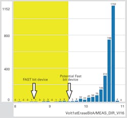
Figure 2 shows a distribution of dies with fast bits in a wafer. To meet its quality standard, ams must be able to guarantee that devices close to the pass/fail threshold will stay good after the specified minimum number of write/erase cycles.
Precise characterization of EEPROM devices
For its foundry customers, ams must be able to characterize production wafers containing EEPROM blocks to filter out failed dies and guarantee the lifetime and data retention of known good dies.
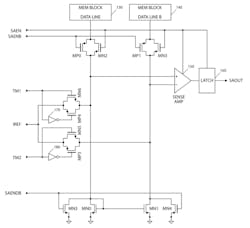
As shown above, characterization of an EEPROM die calls for measurements of input voltage and bit cell charge. And in an EEPROM IP block, these measurements can only be
captured accurately with dedicated test circuitry routed to a
pin (Figure 3).
This DFT circuitry connects the on-chip high-voltage generator in such a way that the voltage needed to program and erase the bit cells may be driven from outside the chip. Once the bit cell is programmed or erased, the bit cell current can be measured on the same pin, accurate to within a few nanoamps. If the charge is below the minimum threshold for guaranteed lifetime, the device will be failed.
This DFT method guarantees that every bit cell in every chip in every wafer will be tested with the same input voltage. By contrast, in the absence of the dedicated test circuitry, the test routine would use the device’s internal charge pump to generate the voltage, and because of process variation, this voltage will vary from one die to another. As a result, the test results will be subject to a degree of uncertainty: A bit cell with a low charge might be a failure in its own right—or it might have been exposed to too low a programming voltage.
The DFT mode implemented by ams eliminates this source of uncertainty, vastly improving the test quality of this block.
Once all bit cells have been programmed or erased, a digital check can be initialized by sourcing an external reference current to the external test-mode pin. The sense amplifier (Figure 3) compares the reference current to the current at the bit cell: If the bit cell current is greater than the reference, a digital high is sent; if the bit cell current is smaller than the reference, a digital low is sent. This produces a digital pattern to verify that all bits are programmed or erased correctly, which may be used to quickly check operation of the device.
Characterizing the device for production
The test mode built into the IP block, then, provides for accurate measurement of the crucial input voltage and cell current parameters, enabling ams to reject dies containing fast bits.
The question then becomes, how can ams guarantee 10 years’ data retention in dies that pass the input voltage and charge tests?
To do so, it tested the performance of dies near the threshold of rejection as a fast bit. It exercised these dies with the maximum number of endurance loops the device was specified to withstand. This gave the test engineers a set of marginal devices that already had reached the end of their guaranteed operational lifetime.
These dies then were baked for 4,000 hours at 250°C. According to the standard Arrhenius equation, this is equivalent to 10 years’ operation at 150°C. After this data-retention bake, the dies were tested to check for drift in the bit cell current. If the cell current was found to have drifted by less than 1 µA, data retention would have been verified. It turned out that all failures were actually triggered within the first 24 hours of baking.
If data programmed on the last write operation of the most marginal device can be retained for 10 years, then the data retention capability of every other known good die can be confidently guaranteed.
Transferring the development test method to production
With the DFT circuitry embedded in the EEPROM IP, the fabrication plant at ams now can characterize every cell in every die in the way described above to screen out fast bit dies. Using the test method outlined here, known good dies with cell current and input voltage values exceeding the minimum threshold may be guaranteed for any number of write/erase cycles and any data retention interval specified by the user of the EEPROM IP block.
The production test method includes a 24-hour bake at 250°C, after which dies showing a cell current drift of more than 1 µA are rejected.
With this characterization program in place, more than 10 million EEPROMs, containing some 300 billion bit cells, have been produced, tested, and shipped to customers. The guarantee of quality supported by this production testing regime has been verified in practice: Not a single device has been returned from a customer, suggesting no failures have been found in the field.
ams could not have verified its test method with sufficient confidence, nor as accurately identified marginal bad devices, without the test modes implemented in the EEPROM IP block’s circuitry. This provides real-world proof of the value of implementing a DFT approach from the outset of a new chip design.
About the authors
Peter Sarson, the test development manager for the Full Service Foundry business unit at ams AG, began his 15-year semiconductor industry career in 2000 when he joined the LTX Applications Engineering Group. He received his Chartered Engineer Status from IET in 2003 and his Chartered Manager status in 2014. Sarson holds a Bachelor of Engineering degree in Electrical and Electronic Engineering from The University of Sheffield.
Gregor Schatzberger is principal analog designer at ams AG. He joined the company in 1998 and since then performed various roles within the BaseIP group of ams. Schatzberger has several patents and has written several papers. He holds a degree in Electronic Engineering from the Technical University of Graz, Austria.
Andreas Wild has been working as marketing manager for foundry services and technologies in the Full Service Foundry at ams since 2003 and also is responsible for customers in the United States and southern Europe. He began his career in semiconductors in 1995 as an administrator responsible for the product engineering laboratory at Austria Mikro Systeme International AG. Wild holds a high school diploma in electronics.
About the Author
Voice Your Opinion!
To join the conversation, and become an exclusive member of Electronic Design, create an account today!

Leaders relevant to this article:


