GaN shows promise for transportation, communications applications
Gallium nitride is a promising semiconductor process for power-electronics devices serving applications ranging from transportation to communications infrastructure. Research into GaN technology, which compared with silicon offers higher breakdown voltages, faster speeds, and lower on-resistance, is proceeding as companies bring practical GaN devices to market.
On the research front, imec, the nanoelectronics research center, announced in May a strategic partnership regarding gallium nitride-on-silicon (GaN-on-Si) technology with IQE, which provides advanced semiconductor wafer products and services. The partnership builds on promising results achieved in a recent project in which imec and IQE collaborated to fabricate GaN power diodes using imec’s proprietary diode architecture and IQE’s high-voltage epiwafers.
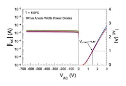
In that project, imec applied its Gated Edge Terminated (GET) Schottky diode device architecture to IQE’s high-voltage GaN buffers on 200-mm Si substrates. Thanks to the GET diode device architecture and the low buffer leakage current of IQE wafers, the large GaN power diodes (10 mm) that were fabricated in imec’s 200-mm Si pilot line showed a low leakage current (at up to 650 V) and low turn-on voltage. The power Schottky diodes reach forward and reverse specifications across the full temperature range, spanning from 25°C to 150°C with a tight distribution (Figure 1). The diodes have 10-mm anode width and an anode-to-cathode distance of 10 µm.
Courtesy of imec
IQE will be participating in imec’s GaN-on-Si Industrial Affiliation Program, which offers joint research and development on GaN-on-Si 200-mm epitaxy and enhancement-mode device technology to a variety of companies including IDMs, equipment and material suppliers, fabless design houses, and packaging companies. The program includes research on novel substrates to improve the quality of epitaxial layers, new isolation modules to enhance integration levels, and advanced vertical device development.
Wayne Johnson, head of IQE’s Power Business Unit, said in a press release, “The importance of GaN-on-Si for power devices cannot be understated, particularly as we enter an era of electrically propelled transportation and increasing demands for energy-efficient power control systems that require high-voltage and high-power capabilities.” Rudi
Cartuyvels, executive vice president for smart systems and energy technology at imec, added that the organization’s 200-mm GaN-on-Si process can be engineered to fit partner-specific product needs.
In related news, IQE announced in May that it has successfully transferred Translucent cREO (for Rare Earth Oxide) semiconductor technology to IQE’s facility in Greensboro, NC (IQE announced an exclusive license of cREO technology from Translucent parent company Silex Systems in September 2015), where a production tool now is producing cREO templates on Si. IQE said GaN-on-Si typically exhibits an undesirable p-type parasitic channel at the GaN/Si interface that detrimentally affects RF efficiency. But using patented technology, IQE said it has demonstrated that the parasitic channel can be completely eliminated.
Dr. Rodney Pelzel, vice president, IQE Group Technology, commented in a press release, “We have demonstrated that we are able to rationally manipulate the cREO characteristics to tune the conductivity of the III-N/Si interface. This is a significant enabler for GaN HEMT technology on Si for RF applications. In addition, it is an enabler for other III-N technology on Si such as RF filter technology.”
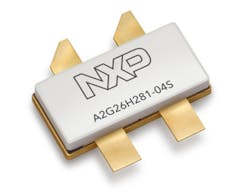
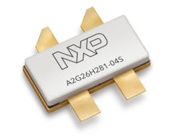
The International Microwave Symposium in May provided a venue for companies to tout the GaN devices they are making for commercial and military applications. NXP, for example, launched an expansion to its portfolio of 48-V GaN RF power transistors (Figure 2) optimized for Doherty power amplifiers for use in current and next-generation cellular base stations, according to Jim Norling, vice president, cellular infrastructure. He added that NXP also has expanded its portfolio of broadband GaN RF power transistors for electronic warfare and battlefield radio applications.
Courtesy of NXP
Qorvo announced, in conjunction with NanoSemi, a developer of digital linearization and compensation algorithms, that it has demonstrated industry-leading ultra-wideband linearization results with its GaN power amplifiers for wireless infrastructure. The demonstration employed Qorvo’s QPA2705 integrated GaN driver and GaN Doherty power amplifier along with NanoSemi’s proprietary digital compensation algorithms.
Sumit Tomar, general manager of Qorvo’s Wireless Infrastructure business unit, said Qorvo’s compact PAs and NanoSemi’s digital-predistortion IP will help customers meet challenges that appear when implementing next-generation base stations such as those having active antenna systems with 64 transceivers—which require small form factors, high efficiency, and linearity to support multicarrier configurations.
Wolfspeed offered live product demonstrations at IMS. One centered on the CGHV14800, a high-power GaN HEMT device designed for L-Band radar applications. Another employed the CGHV59070 GaN HEMT for C-band radar systems. Yet a third demonstration showcased a wideband LTE Doherty power amplifier developed using the company’s high-performance 0.4-µm 50-V GaN RF foundry process.
Ryan Baker, product marketing manager for RF components, cited a milestone the company has reached. As of the end of 2015, he said, Wolfspeed had shipped GaN-on-SiC RF power transistors with a combined RF output power of more than 1.3 GW (sufficient to power 124,900 U.S. residential homes for a year).
About the Author

Rick Nelson
Contributing Editor
Rick is currently Contributing Technical Editor. He was Executive Editor for EE in 2011-2018. Previously he served on several publications, including EDN and Vision Systems Design, and has received awards for signed editorials from the American Society of Business Publication Editors. He began as a design engineer at General Electric and Litton Industries and earned a BSEE degree from Penn State.
Voice Your Opinion!
To join the conversation, and become an exclusive member of Electronic Design, create an account today!

Leaders relevant to this article:


