Communications Timing: Pruning clock-tree problems

The interpretation of signals within a synchronous digital communications system relies upon timing. Whether a 1 or a 0 is read by a receiver depends entirely on when the signal is sampled, and sample timing is controlled by the system clock. So, it’s not surprising that a great deal of attention is given to generating and distributing clock pulses.
Jitter in the time domain
Variation in clock edge position is called jitter and can be defined in several ways. Cycle-to-cycle (C2C) or period-to-period jitter is the difference between measurements of the time from one clock rising edge to the next. Period jitter refers to the variation in clock period relative to the ideal—often a computed waveform. Time interval error is the deviation from the ideal position for clock edges relative to a reference position.
A test procedure to determine the C2C jitter is relatively straightforward although tedious if attempted manually. As described in an SiTime white paper, “C2C jitter is defined in JEDEC Standard 65B as the variation in cycle time of a signal between adjacent cycles, over a random sample of adjacent cycle pairs. The JEDEC standard further specifies that each sample size should be greater than or equal to 1,000.”
The reference sets out a suggested procedure:
- Measure the cycle times of two adjacent clock cycles, T1 and T2.
- Calculate the value of T1-T2. Record the absolute value of this number.
- Wait a random number of clock cycles.
- Repeat the above steps 1,000 times.
- Compute the standard deviation and the peak value from the 1,000 samples.
- Repeat the above measurements 25 times and calculate the average peak value from the 25 sets of results.1
Only the first five steps are needed to find an accurate RMS level. However, because of the random nature of jitter, the peak value will continue to increase as more measurements are taken. Reference 1 suggests that measuring 25,000 pairs of randomly chosen cycles will include enough of the large infrequently occurring values to provide confidence in the final peak-to-peak value.
Some types of jitter require 1,000 measurements, and others need 10,000 to calculate an RMS quantity. In either case, the peak-to-peak value should be determined from a much larger sample size. From a table in Reference 1 that listed standard deviation vs. sample size for a Gaussian distribution, the peak-to-peak jitter should be about 7.44x the RMS value if 10,000 samples are taken—about 9.51x RMS if 1,000,000 samples are used.
Long-term jitter is a cumulative measurement made over 10,000 contiguous cycles rather than random ones. This value also is called accumulated jitter and, according to the reference, is useful in graphics/video displays and long-range telemetry applications such as range finders. SiTime makes a range of MEMS clock generators with stability in the ±20-ppm range to replace crystal oscillators in many applications.
A Silicon Labs white paper discusses the additional jitter that a clock buffer contributes and makes a strong link between jitter and slew rate. For the company’s Si53301 2.5-V LVDS buffer running at 156.25 MHz, the paper concludes that a slew rate faster than about 0.6 V/ns gives optimum results.
This reference recommends, “… to maximize the input slew rate it’s best to locate the clock driver as close to the source as possible, use a differential input, which effectively doubles the slew rate—plus has the advantage of common-mode noise rejection—maintain a full-level input swing (do not attenuate the input unless maximum levels are exceeded), and optimize impedance matching as reflections will also degrade input slew rate.”2
Frequency-domain phase noise
Phase noise is the frequency-domain equivalent of time-domain jitter. Reference 3 comments that, “… the best frequency-domain instruments have a lower noise floor than the best time-domain instruments. This fact makes frequency-domain equipment the instruments of choice for ultra-low phase-noise clock signal measurements that are free of data-dependent jitter.”
As noted in a phase-noise tutorial, “… oscillators used for sampling clock generation are more often specified in terms of phase noise rather than time jitter.”4 This observation specifically related to ADC clock sources but generally applies to clock oscillators used in digital communications.
For example, Figure 1 shows the phase noise for the Analog Devices’ ADF4360-1 2.25-GHz PLL with a 10-kHz loop filter. The area A for any one trapezoidal section is the integrated phase noise power, and the equivalent RMS jitter in seconds is given by
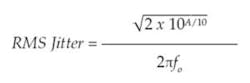
where f0 = oscillator frequency.
For the example in the figure, each trapezoidal area A—equal to the width multiplied by the sum of the two heights divided by two—was separately evaluated and the jitter calculated. Then all the jitter contributions were summed as a root-sum-square calculation because the separate parts were considered to be uncorrelated.
A problem that can arise from this technique is the assignment of the upper and lower integration frequency offset limits. Reference 2 explains, “The integration bandwidth used for the jitter calculation … has a great impact on the measured jitter performance. The integration bandwidth of interest will depend on the application. If in doubt, be sure to use the same bandwidth when making comparisons. The most common bandwidth used is 12 kHz to 20 MHz.”
Courtesy of Analog Devices
The PLL associated with Figure 1 could be driving an ADC with a much wider bandwidth of its own. Because of the 10-kHz loop filter, the clock noise bandwidth is limited, and it’s obvious that extending the upper integration limit from 100 kHz to 100 MHz only adds a small amount of jitter. This would not be the case if the ADC clock were not band limited, and the upper integration limit would have to be chosen more carefully—it could extend all the way up to the ADC’s clock bandwidth. Reference 5 includes a good discussion of upper and lower limit selection.
Clock manipulations
Phase noise
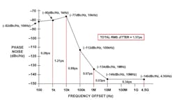
You could avoid many jitter-related problems by buying the best available oscillator. A much less expensive approach is to use a jitter-cleaning device such as Analog Devices’ AD9523-1 dual-loop clock generator. In Figure 2, a simulation using the company’s ADIsimCLK tool shows the device generating 983.04-MHz clock outputs.6
Courtesy of Analog Devices
The first PLL has a very small bandwidth, which means that it cannot respond to rapid changes—in this case, the reference input’s short-term jitter. So, the output of the first PLL has the same frequency as the reference input clock but lacks most of the reference’s jitter. Instead, the 122.88-MHz input to the second PLL has the much lower phase noise of a good quality crystal oscillator.
As Figure 2 shows, separate internal paths allow two related clocks to be generated and distributed to several outputs. In the figure, the same divisor was used for each group of clocks, but changing the value to 4 or 5 results in output frequencies of 737.28 MHz or 589.82 MHz, respectively.
Additional flexibility is available in the form of programmable dividers and delay elements for each of the 14 complementary outputs. As described in the device datasheet, “Each divider is programmable with 10 bits of division depth that is equal to 1 to 1,024. Dividers have duty-cycle correction to always give a 50% duty cycle, even for odd divides…. The dividers support programmable phase offsets from 0 to 63 steps, in half periods of the input clock (for example, the VCO divider output clock).” Finally, the polarity and strength of each of the 14 output drivers are separately programmable, so one can be driving a LVDS device and another some LVPECL logic.
Skew
Within a clock chip such as the AD9523-1, timing differences are minimized by design. The device datasheet quotes a worst-case 50-ps skew among the 14 outputs. That’s measured at the chip pins, so the individual clock paths and loads all need to be identical if the initial skew is to be preserved. Generally, this isn’t practical, and some additional amount of skew accumulates because of the way each output is routed to the load(s) it drives and the variation of capacitance among the loads.
What if you need a clock edge to have virtually zero delay from the reference clock? A clock buffer, the connection to it from the reference source, and the connections from the buffer to the loads it drives all add delay. The trick is to use a PLL that effectively advances its output to offset the delays. The result is an output with apparently zero delay.
What’s actually happening is that the delays in the system have been adjusted so that edge 1 of the reference is being lined up with edge 2 of the PLL output. Several companies make so-called zero-delay buffers, which can solve difficult clock distribution problems. A Cypress Semiconductor application note discusses the roles of capacitive loading and trace length in determining whether one clock signal lags or leads another at the driven loads. Only one clock can be fed back to the PLL to force that signal to be aligned with the reference. All the other clock paths must be designed relative to the zero-delay output.7
Several manufacturers provide zero-delay PLL-based clock buffers that are compatible with spread-spectrum techniques. Spread-spectrum modulation adds a small amount of periodic variation to the clock frequency. This sounds counterintuitive when the amount of effort to generate a very low phase-noise signal is considered. However, the peak EMI associated with a single narrow tone will be higher than if the same power is spread over a wider frequency band. Spread-spectrum techniques do this, and a Cypress white paper comments that EMI reduction of several decibels can be expected, with the greatest improvement occurring at higher harmonics.8
Although a PLL with a low loop-filter bandwidth may reduce the regenerated clock jitter, the output cannot follow the cycle-to-cycle timing changes caused by spread-spectrum modulation. A Cypress Semiconductor website Q&A page includes the following reply to a question about using a PLL-based zero-delay buffer with spread-spectrum modulation. “The CY2305 and CY23S05 are newer design parts. The only difference between the two would be the spread-spectrum compatibility: CY2305 is not spread-spectrum compatible. CY23S05 is spread-spectrum compatible with wider loop bandwidth.”
Several companies in addition to Cypress make clock buffers designated as “2305”—Integrated Device Technology (IDT), ON Semiconductor, and Silicon Labs, among others—but the device characteristics are not designated in the same ways by variations in the part number. The SL2305NZ from Silicon Labs and ON Semiconductor’s NB2305A are zero-delay parts, but IDT’s 2305NZ is just a straightforward five-output buffer with no PLL. IDT’s 2305 without the NZ suffix is a zero-delay part. So, some care must be exercised when specifying equivalent devices.
Getting help
Clock tree design can be daunting. Especially for relatively large systems with high frequencies and tight tolerances, there can be a lot of moving parts to coordinate including the reference oscillator, spread-spectrum modulation, buffering, and load equalization. Accounting for external clock tree layout effects as well as device-specific timing skews and offsets requires detailed simulation.
The free online Texas Instruments WEBENCH Clock Architect tool uses TI components to design a range of complete clock distribution trees starting from the required input and output frequencies. The tool determines the approximate cost of each proposed solution as well as the area of the parts used, the current drawn, the phase noise and jitter, and the component values needed for the PLL loop filter.
IDT offers both complimentary clock tree design as well as a design review service. The IDT website cautions, “Clock tree design can be a complex task with many considerations that are often overwhelming to designers unfamiliar with clock trees and the associated ‘language’ of timing. While clock tree tools and wizards sometimes exist to assist with simple clock tree designs, these often fall short in real-world applications; automated tools simply can’t address many of the complexities of advanced requirements like phase jitter and spread-spectrum.… Our in-house experts can assist you in building a new clock tree from the ground up or evaluating and improving an existing clock tree design.”
You can choose where you want to start with the free online Clock Tree Expert tool from Silicon Labs. Are you an expert, or do you want to be guided through the design process by a wizard? Either way, the tool helps you design a clock distribution network based on Silicon Labs products.
Analog Devices also provides a free online clock design tool. As described on the company’s website, “ADIsimCLK is the design tool developed specifically for Analog Devices’ range of ultra-low jitter clock distribution and clock generation products.… ADIsimCLK will enable you to rapidly develop, evaluate, and optimize your design.”
Features include:
- jitter performance—broadband and SONET specifications;
- phase noise performance;
- phase noise impact—ACI/ACR, EVM, phase jitter, etc.;
- jitter impact on ADC performance—SNR, ENOB; and
- accurate timing analysis (logic analyzer display).
ADIsimCLK models PLL frequency synthesizers with external VCOs as well as integrated PLL/VCOs. The tool includes phase noise analysis with reference, VCO, loop filter, and phase detector contributions as well as nonlinear transient analysis for accurate determination of lock time.
References
- Clock Jitter Definitions and Measurement Methods, SiTime, SiT-AN10007, January 2014.
- Understanding and Optimizing Clock Buffer’s Additive Jitter Performance, Silicon Labs, AN766, April 2013.
- Clock Division with Jitter and Phase Noise Measurements, Silicon Labs, July 2015.
- Kester, W., Converting Oscillator Phase Noise to Time Jitter, Analog Devices, MT-008 Tutorial, October 2008.
- Neu, T., “Clock jitter analyzed in the time domain Part 1,” Analog Applications Journal, Texas Instruments, 3Q 2010.
- Slighton, K., “Dual-Loop Clock Generator Cleans Jitter, Provides Multiple High-Frequency Outputs,” Analog Dialogue, January 2014.
- Understanding Cypress’s Zero Delay Buffers, Cypress Semiconductor, Application Note AN1234, 2014.
- Shah, B., EMI and Spread Spectrum Technology, Cypress Semiconductor, White Paper 001-71991, August 2014.
For more information
About the Author

Tom Lecklider
Comment About the Article
To join the conversation, and become an exclusive member of Electronic Design, create an account today!

Leaders relevant to this article: