Laser Selective Soldering: Process under control for automotive applications
The laser is based on a phenomenon discovered during the past century, and laser technology became real and concrete at the beginning of the 1960s. In less than 50 years, it has become the basis for numerous applications that today have reached high levels of sophistication, including the laser soldering of electronics.
Laser background
By way of background, broadly speaking, by adopting appropriate materials and precautions that take advantage of certain laws of physics, it is possible to produce what is commonly designated as a laser beam—a well-defined electromagnetic wave. However, a laser beam is not a common electromagnetic wave but rather radiation with the characteristic of providing a coherent flow, both from space and time perspectives. It is from this flow that the beam derives two important aspects:
- The first is to be monochromatic—characterized by a very restricted set of wavelengths which, depending on the type and the materials used, may range from infrared to ultraviolet.
- The second is to be collimated—made up of a set of parallel, unidirectional subelements.
Specifically, the second property—collimation—results in the capability of the laser to convey energy with a much higher density (energy/surface area) than a standard light source.
In other words, a laser source can be considered as a source of energy capable of injecting energy without direct contact with the target and on very small and defined areas.
Selecting the appropriate wavelength of the source enables the optimization of the laser beam, according to the process and materials involved, to achieve the best transmission and absorption of energy by the target.
A laser beam can be conveyed from the output of the source either via optical fibers or by means of a system of mirrors. The mirrors can be either fixed or movable, actuated using galvanometers, to deflect the beam where necessary.
Finally, an essential element of the laser transmission chain toward the target is the optics, whose task is to focus it on the desired point and in the desired manner.
Technologies for electronic board assembly
In the development of technologies related to electronic components and board assembly, the last 20 years have seen the gradual decrease of through-hole technology (THT) components in favor of surface-mounted devices (SMDs). It is a point of fact that the advantages of the latter technology are innumerable, and we will not discuss them here. But the reality is that, although sought by many, the complete elimination of THT components and technology has never taken place.
Anyone assembling electronic boards is aware of the need to cope with the issues of mounting and soldering some THT components on the board precisely and often very quickly, especially in case of high-volume production. This must be done without damaging what is already mounted on the board and without compromising the quality of the assembly, which up to that point has undergone less critical assembly processes, designed for high throughput.
In addition, more recently it has become increasingly common to design objects consisting of one or more electronic boards inserted into plastic housings. In this case, electronics and plastic often are joined by means of metal tabs that make the mechanical and electrical connections between the parts. These tabs must be inserted and soldered between the different elements of the assembly in the same way as THT leads.
Laser and selective soldering in the automotive sector
In the automotive industry, production volumes generally are high, as are expectations in terms of yield and quality. Design and integration requirements often mandate the assembly of the electronics in external housings with shapes that are difficult or impossible to handle inside traditional soldering systems. The high production rates impose continuous manufacturing cycles where automation becomes essential to respond effectively. The incessant demands for cost reduction leave no room for the use of excessively complex and/or expensive customizations. Finally, time-to-market requirements do not leave any time for design reviews aimed at increasing manufacturability of assembly by implementing more traditional technologies.
From what has been discussed so far, it is easy to understand that a laser has some intrinsic characteristics that make it a very interesting technology to implement in the selective soldering process for the completion of assembled electronic boards. In particular:
- it does not require direct contact with the solder joint,
- it has the agility to access boards with severe issues of accessibility and proximity of adjacent components,
- it can be applied on boards where the bottom side is facing upwards (which is not uncommon in some automated lines),
- it enables modulation of the amount of energy and its surface distribution based on the specific point involved, and
- it offers the flexibility to adapt to different production requirements without requiring additional equipment.
Laser and selective soldering for electronics
When setting out to design this type of system, it is mandatory to take into account a series of issues, some of which may be resolved in the design phase and others on the basis of data collected during experimentation.
Let us analyze first the laser source, which provides all of the energy for the process.
The semiconductor lasers available on the market today can supply adequate power and wavelengths. Powers in the range of 60 W (nominal continuous) have proved to be the most suitable for the soldering process. This power level can easily heat even a significant metal mass as well as melt the filling material; wavelengths in the range 970 nm to 1,064 nm have been found to be the best in terms of minimizing reflection and achieving good, constant absorption of energy by the materials to be joined.
However, it is necessary to check other relevant aspects such as, for example, the correct uniformity of the flow output from the optics. Otherwise, the heating of the soldering area may not be uniform, opening the door to uncontrolled variables that can impair the quality and repeatability of the process.
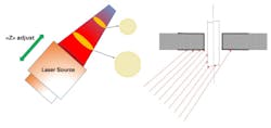
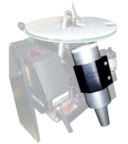
The beam output from the source, which is theoretically cylindrical with Gaussian distribution, is connected to the optics via optical fiber. This fiber must be carefully selected with the goal of correcting aberrations between the theoretical beam and the real beam, which vary depending on the type of source used. The fiber also needs to transform the beam from cylindrical to conical (Figure 1) to be focused during execution of the soldering program. The focus point must be variable in order to accommodate the process requirements. By changing the distance between the optics (Figure 2) and the target, it is possible to define the diameter of the laser beam on the surface to be heated, effectively determining the intensity of the energy applied.

Like any brazing process, the laser soldering method must implement specific stages that constitute a real temperature profile: preheating of parts, melting of the filling material, activating the fluxing agent, maintaining the liquid state to ensure the correct wetting, and forming the proper thickness of intermetallic bond, necessary not only to ensure electrical continuity but also, above all, to achieve the adequate level of mechanical strength of the solder joint.
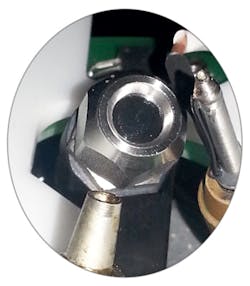
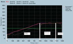
The quality of the solder joint strongly depends on how this profile is implemented and maintained over time. To verify this, a sensor able to provide continuous feedback regarding the temperature of the soldering point should be included in the system. For this reason, along with the source and related optics, the laser selective soldering system should integrate an accurate optical pyrometer (Figure 3), which enables monitoring of the temperature of the solder point and the adjustment of power, intensity, and time during debug of the program to define and maintain the correct values (Figure 4).
Since the intensity of the applied energy depends on the power generated by the source as well as on the surface where this power is distributed, it is essential to be able to monitor these parameters point by point. The instantaneous power output by the generator is a factor which is easily managed by the control unit.
On the other hand, to control the surface of application in a repeatable and continuous manner, it is necessary to always know the exact height at which the PCB is located, compensating for any deformation and/or warpage caused during preceding thermal processes.
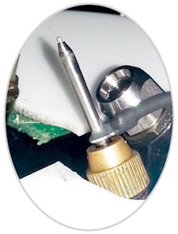
This is why it is essential that the soldering system be equipped with a sensor capable of measuring the actual distance between the emitter optics and the board surface (Figure 5). This is the only way to accurately ensure that the Z height programmed to define the correct energy application pattern is constantly maintained for each board.
Finally, consider the filling material. A wire containing a no-clean fluxing agent is used; today, formulations designed specifically for laser soldering are available. Both lead and lead-free processes can be implemented. Managing the filling alloy is a delicate stage: The programmer should be able to define the exact filling time, the amount, and the direction from which the wire is supplied. It also should be possible to change this direction, even during the filling stage, to be able to circle around the lead to improve wetting and reflow where necessary.
To perform this stage correctly, the system should be equipped with a dispenser that, by unrolling the wire from a spool, can accurately deliver it on the brazing point.
For this purpose, it should be noted that, to attain perfect process repeatability, it is important that the system be able to accurately dole out the amount of wire supplied by measuring the length of the wire rolled out for each solder joint. Since the tip of the wire is the result of a previous soldering, it is never at exactly the same distance with respect to the board. The wire dispenser must take this aspect into account to compensate, avoiding an otherwise inevitable error in the amount of wire supplied to the joint (Figure 6).
Lastly, consider the board surface finish. The practical experience resulting from years of testing led to the conclusion that the most suitable finish for best results is hot-air leveling. This is due to the fact that this coating also is very tolerant with respect to how it is stored. Chemically deposited tin provides good results as well as the nickel-gold coating which, as a result of increased reflecting properties, requires higher power applied for a longer time.
In addition, the copper organic solderability preservative coating, even though less expensive and technically usable in a laser soldering process, also is the most critical in terms of process stability, since it is significantly affected by imperfect storage conditions and preceding thermal processes.
Design for laser solderability
Despite its advantages and unmatched flexibility, laser soldering for electronics is not free of issues or areas of nonapplicability.
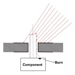
An incorrect board design, for example, where the hole and component lead diameters are not correctly sized, may lead to burning of or damage (normally external) to the body of the component located on the opposite side of the board. In this case, the laser light, which enters the excess space between the hole and lead, may be reflected by the internal plating, causing it to exit on the opposite side, hitting the component (Figure 7).
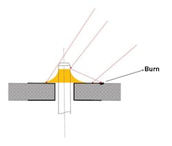
Also, under certain conditions, the laser light may be partially deflected by the lead and by the solder joint during formation, resulting in burning, normally on the pad edge (Figure 8).
Other critical process aspects can arise when, due to an error during the board layout process, bottlenecks to minimize thermal diffusion were not included, or when the lead to be soldered is located on a trace connected to large power planes, which can absorb huge amounts of heat during the soldering process. Generally, these issues can be minimized by adopting a series of precautions at the design stage.
Conclusions
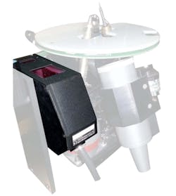
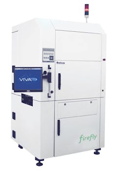
Laser soldering in the electronics and automotive industries is a technology that can be of great help in solving manufacturing issues where there are high volumes and high quality expectations. A laser selective soldering system (Figure 9) must be easy to integrate into automated lines and able to operate from either the top or bottom side of the assembly to be soldered; in some cases, applications on both sides have been implemented.
These systems can feature a reduced footprint, and their control mechanisms ensure a high uptime with a minimum of maintenance and inspection activities.
Another positive aspect of the technology is related to energy consumption. A laser soldering system is a low-consumption option (generally 2.5 kW max.), since there are no alloy baths to be maintained in the liquid state. These systems are extremely safe for operators, ranked as Class 1 (the same ranking as a domestic CD player), thanks to the integrated safeguards and protections.
About the author
Alberto Ghirelli is a key account manager at Seica. After completing electrotechnics/electronics studies in Milan, Italy, Ghirelli spent the first years of work within the hardware and microprocessor firmware development area on industrial and military projects. In the mid 1990s, he moved within the assembled PCBs industry and, for more than 20 years, has worked on equipment and technologies for electronics manufacturing, production, inspection, and testing.
About the Author

Comment About the Article
To join the conversation, and become an exclusive member of Electronic Design, create an account today!

Leaders relevant to this article: