Field failures of electronic components or modules often are initiated by unintended gaps within the component or module. The gaps may be referred to as nonbonds, cracks, delaminations, or voids. They typically are filled with air or another gas. They cause unanticipated field failures by expanding through thermal cycling, through corrosion, or through both of these mechanisms.
In development, production, and failure analysis, it often is necessary to determine whether any of these anomalies are present, and, if they are, to characterize their importance. An air-filled anomaly that is relatively thick—a large bubble-like void, for example—may be found by X-ray. But because electronics components and modules tend to have layered structures, these anomalies are likely to be very thin. That makes them good subjects for an acoustic micro-imaging tool, which can detect and image gaps as thin as 200Å.
When the scanning transducer of an acoustic micro-imaging tool launches a pulse of ultrasound into a sample, virtually 100% of the ultrasound is reflected back to the transducer if the pulse has struck the interface between a solid material and air or another gas. The returning echoes therefore have very high amplitude and are imaged as bright white pixels that contrast strongly with the surrounding nongap regions of the acoustic image. Echoes from interfaces between two solids have lower amplitude and, in monochrome images, gray pixels.
This description fairly well describes what is called the reflection mode of acoustic micro-imaging, more technically known as C-Mode imaging. In all, there are more than a dozen imaging modes, many of them developed by Sonoscan. Each makes use of ultrasound in its own way. In reflection mode imaging, the operator gates the return echoes on a depth of interest—meaning that only echoes from within a vertical range representing the depth of interest are used in making the acoustic image while echoes coming from material interfaces above and below the gated depth are ignored.
A reflection mode image is two-dimensional, even though it represents a three-dimensional target zone. In many applications, the two-dimensional view is adequate: The operator needs to know only that a defect is present and not its precise depth, or the operator can correctly deduce the relative depth of a defect from surrounding features whose depths are known.
But when more needs to be known about the Z-dimension extent of a crack, delamination, or other feature, a quick and accurate method is to use simultaneously not one but two acoustic imaging modes: the THRU-scan mode and the multigate mode, both developed by Sonoscan for its C-SAM acoustic micro-imaging systems.
THRU-scan does not collect acoustic reflections from material interfaces. Instead, it uses the transducer and a second sensor positioned below the sample and perfectly aligned with the transducer. As the transducer above the sample scans, it sends thousands of pulses of ultrasound into the sample each second. Some pulses will encounter only one or a few mildly reflective interfaces; most of the ultrasound will exit the bottom side of the sample and be recorded by the sensor there. This ultrasound will look fairly bright in the THRU-scan image. Other pulses will encounter more reflective or absorbing features and will be somewhat darker. And some pulses will encounter interfaces (solid to air in a gap, for example) that reflect essentially all of the ultrasound to the transducer. Features of this type will be solidly black in the thru-scan image. THRU-scan is a fast and easy way to identify and image any gap-type feature (as long as it does not lie directly below another gap-type feature). The THRU-scan image, however, gives no measurement information about a gap’s depth in the sample.
The multigate reflection mode takes advantage of the fact that echoes reflected from interfaces at different depths arrive at the transducer above the sample at different times. Ultrasound travels through different production materials at different speeds—through silicon at around 8,000 m/s, for example, and through mold compounds at around 3,000 m/s. The travel time from the reflecting interface inside the sample to the transducer above the sample is measured in nanoseconds. The system operator can specify the number of gates and their vertical extents and positions. The gates usually are all of the same vertical thickness and usually are adjacent, but if required they may be of varying thicknesses and be separated vertically. Each gate will produce an acoustic image of the depth it covers. Scan time is the same as it would be for the reflection mode.
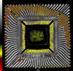
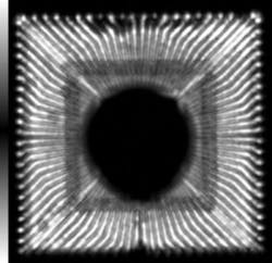
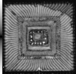
Figure 1 is the THRU-scan image of a plastic quad flat pack (PQFP). The ultrasonic signals were collected by the sensor scanning the bottom side of the component; the effect is that one is looking, acoustically, upward through the bottom of the PQFP. The outlines of the die, the die paddle, and the lead fingers are all visible because they transmitted downward some portion of the ultrasound launched by the transducer above the component. The black circular feature in the center is the acoustic shadow of an air-filled anomaly that is more or less centered on the die. The depth at which it lies, however, cannot be determined from a thru-scan image—the anomaly could be above or below the die.
Sonoscan’s multigate mode was used at the same time to image a sequence of 10 gates, starting at the top surface of the component. The gates were adjacent to each other, and each had a vertical extent of 0.206 mm. The images of gates #1, #2, #3, and #4 are not shown here: gate #1 was featureless and white because it included the surface that reflected ultrasound. Gates #2, #3, and #4 were completely black because the vertical extent of each of these gates encompassed only mold compound having no internal features such as voids; there were no features that could reflect ultrasound.
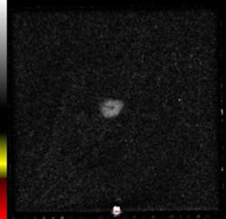
The multigate image of gate #5 is shown in Figure 2. The small rounded feature in the center appears to be the top portion of a feature or defect that intrudes only slightly into gate #5 from below. It also is positioned about at the X-Y center of the die. (The small white feature in the bottom center is a chipout at the top surface of the component package.)
Figure 3 is the acoustic image of gate #6. The vertical extent of this gate includes the distal ends of the lead fingers, many of which are red because they are delaminated on their top sides from the mold compound. The outline of the die now is visible because the outer part of the coating on the top surface of the die is red, meaning that it is delaminated from the die. The gray region at the center of the die appears to be the rest of the die coating; its appearance in the gate above this depth suggests that it has not merely delaminated from the die but has actually popped upward.
Figure 4 is the next gate down (#7). At this depth, the gate is partly below the popped-up die coating, with the result that some of the more or less linear structures in the image of the coating now are black acoustic shadows created by ultrasound reflected from below. The top surfaces of all of the lead fingers appear to lie within this gate and have abundant delaminations (red) from the mold compound.
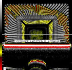
Figures 2, 3, and 4 suggest that the uplifted die coating has a domed shape. To view the dome acoustically from the side, a third Sonoscan mode, called Q-BAM, was used, one that scans not the whole area of the device but only the length of a single straight line selected by the operator. Moving back and forth along this line, the transducer begins at the bottom of the target and gradually moves upward until it reaches the top surface and has collected the acoustic data to create a nondestructive cross-sectional image.
The scan line is marked at either end by the green arrows in Figure 5. The cross section at the bottom of Figure 5 shows the side view of the die coating: it is indeed domed. In addition, the varied shades of red and yellow suggest that it has varying thickness and that the linear features suggested in Figure 3 and seen more clearly in Figure 4 are wrinkles in the uplifted die coating.
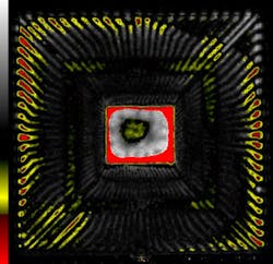
Figure 6 skips down to gate #10. The numerous white features within the outline of the die are voids in the die attach. The uplifted die coating is visible at the center of the die. Except for those in the upper right corner, all of the lead fingers have the same color—very different from what is seen in Figure 5. The explanation is that the lead fingers do not all occupy the same plane because the lead frame itself is bent.
The capability to use two acoustic micro-imaging modes—thru-scan and multigate—simultaneously allows the operator to view the sample from both the top and the bottom surfaces, to identify all internal structural defects, and to identify the specific depth of defects and other internal features. The PQFP illustrated here required only 10 gates; when very thin gates are needed, 100 or more can be set.
About the author
Tom Adams is a freelance writer and photographer who has written more than 500 articles for semiconductor and microelectronics trade magazines.
About the Author
Tom Adams
Consultant, Nordson SONOSCAN
Tom Adams is a professional science writer based in New Jersey.
