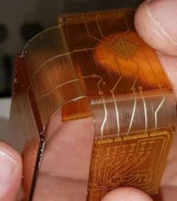
Nano Dimension 3D-prints rigid PCB with flexible conductive connectors

Ness Ziona, Israel. Nano Dimension announced today that it has successfully 3D-printed a series of multilayered rigid PCBs, connected through printed flexible conductive connections. This process provides a solution to traditional production limitations in the electronics industry with regard to factors such as continuous transfer of conductors between circuits, loose contacts, size of connections between the circuits, and fabrication of multilayered flexible material. The process enables the bending of the PCB so that it can be combined with curved and complex geometrical products.
In addition, Nano Dimension has developed unique software that allows the printing of electronics-design files with flexible connections. The software receives complex three-dimensional files (CAD) from the user and converts them, using a unique algorithm, to files that can be 3D-printed.
Printing flexible connections eliminates the need to manually connect the circuits, enabling potential customers to benefit from high-quality connections with favorable mechanical properties with regard to bending, twisting, and strength, while saving space and money.
To the best of the company’s knowledge, Nano Dimension is the first in the world to successfully print multilayered rigid circuits with flexible connections.
According to a recent report from Research and Markets, the global flexible electronics market is anticipated to grow at a CAGR of 25% from 2016 to 2022. The market has generated revenue of $5.42 billion in 2016 and is anticipated to reach $20.67 Billion by 2022. The potential market for this solution includes companies from a variety of industries, such as aerospace, missiles, aviation, flexible electronics, wearable equipment, and the IoT.
One example of how such circuits may be used is during the process of creating a flexible watch. The electronics in the watch could potentially be printed using Nano Dimension’s technology, eliminating the need to manually add connectors. Thus, the watch could be thinner, more durable, and with flexibility properties that vary according to the ergonomic design of the watch.
About the Author

Rick Nelson
Contributing Editor
Rick is currently Contributing Technical Editor. He was Executive Editor for EE in 2011-2018. Previously he served on several publications, including EDN and Vision Systems Design, and has received awards for signed editorials from the American Society of Business Publication Editors. He began as a design engineer at General Electric and Litton Industries and earned a BSEE degree from Penn State.
Comment About the Article
To join the conversation, and become an exclusive member of Electronic Design, create an account today!

Leaders relevant to this article: