Tools extend from DFT software to X-rays
Printed-circuit-board test and inspection becomes challenging as component sizes shrink and access disappears. Solutions include design and DFT software; probes and fixtures; in-circuit, flying-probe, and functional test; and optical and X-ray inspection as well as computed tomography. IPC Apex Expo 2017 scheduled for Feb. 11-16 in San Diego will provide a deeper look at the available tools.
Commenting on the challenges, NK Chari, marketing director, manufacturing technologies, Keysight Technologies, said, “Over the years, we have seen varying customer needs—the latest trend being test asset utilization.” Keysight addresses this trend with a product portfolio consisting of both hardware and software to enable users to leverage different mix-and-match options to achieve complementary test coverage. “For instance, the set of tools that is used to deploy boundary-scan methodologies in NPI must also be relevant for production testing as well,” Chari said. “At Keysight, we offer a complete integrated ICT portfolio solution backed by our strong experience, innovation, global outreach, and comprehensive ICT product library our customers can assess and leverage.”
John Arena, product line director at Teradyne, said, “In high complexity servers and routers, physical access for test probes remains a problem.” Teradyne’s solution is the TestStation, which can support up to 15k physical test points while also supporting access using temporary scan-based test components inserted into empty memory or processor sockets. Providing virtual access of added board nets via scan can cover thousands of additional test points, Arena said, adding, “By combining physical and virtual test point coverage, TestStation can provide high levels of defect coverage for complex PCBAs.”
Scott Manty, director of U.S. sales and business development for Xcerra’s Everett Charles Technologies division, addressed the fixturing aspect of electrical PCB test. He said, “The key challenges facing customers and suppliers … is the ever-changing technology related to printed circuit board size and the electronic components using up board real estate.”
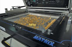
The smaller pad sizes and reduced spaces drive ECT to develop solutions such as special MetriX designs for close center probing of loaded PCBs, providing test access down to 39-mil (1 mm) centers and 18-mil-diameter targets. In addition, he said, “Our Zoom Fixture designs can increase test access on 0.388-mm (0.015-inch) targets with 0.6-mm (0.024-inch) spacing” (Figure 1). The industry standard for conventional fixtures, he added, specifies 0.018-inch (0.46-mm) targets on 0.039-inch (1-mm) centers.
Courtesy of Xcerra’s Everett Charles Technologies division
Fixture costing and turnaround times have become just as critical as technical test solutions, he said, adding that ECT has developed standardized fixture kits that enable a low-cost manufacturing solution. In addition, ECT offers a mass interconnect product line that complements its in-circuit and functional test fixtures.
From DFT to inspection
PCB quality depends on a variety of technologies, extending from DFT software to inspection. According to a Goepel spokesperson, “Each new generation of products increases the problem of physical test access. This has led in recent years to a strong demand for embedded validation, test, debug, and programming solutions, but also for new methods of inspection. With our new inspection systems and our technologies for Embedded System Access, GOEPEL electronic offers groundbreaking test solutions, which can be linked together to improve test coverage and process management.”
The spokesperson added, “For electrical test there is an unbroken trend to integrate more and more test and programming functions directly into the target and to use these features during the entire product lifecycle.” IoT is a key driver of this development. “While JTAG/boundary scan is still doing a great job for structural test, there is a strong market demand to combine it with complementary technologies for embedded functional test and high-speed programming,” the Goepel spokesperson said.
XJTAG focuses on boundary scan. “Testing today’s high-complexity, high-density circuit boards is often time-consuming and expensive, and physical access to many chips is impossible with probes or fixtures alone,” said a spokesperson for the company. “Boundary scan addresses this problem by providing access to compliant ICs on a PCB using a JTAG chain, but it is imperative that any potential errors in the JTAG chain are corrected early in the design cycle.” The company’s XJTAG DFT Assistant allows engineers to determine whether JTAG chains are correctly connected and terminated during schematic capture so that any mistakes can be resolved early in the design process, before hardware is produced.
Apex Expo 2017
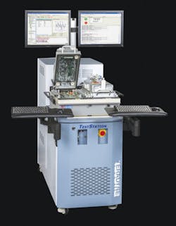
Apex Expo 2017 will offer a venue for vendors to demonstrate their products and technologies. Arena at Teradyne said the company will exhibit its TestStation Multi-Site test system (Figure 2) and automation solutions, “… which provide electronics manufacturers with reliable, high-quality PCBA testing at the highest fault coverage rate without sacrificing throughput. The TestStation platform is configurable to perform manual, robotic assist, or full inline automation for the latest circuit board assembly technologies that are used in automotive, industrial, computing, consumer, communications, and defense end-products.”
Courtesy of Teradyne
Arena said TestStation systems are scalable, allowing users to configure test features to match their specific needs. They can satisfy throughput and budget requirements by replacing two to four conventional board test systems while delivering parallel device programming, in-circuit testing, and functional pre-screen. In addition, he said, “TestStation systems share a common test architecture with consistent hardware options and software environments across system models, allowing users to quickly acclimate across testers to reach maximum productivity.”
Arena also commented on high-reliability automotive/industrial applications, for which meeting parts-per-billion requirements is a challenge. “Teradyne conquers this demand with our TestStation Multi-Site models, which support volume panelized PCBA testing and automated handling to provide no-touch production test of high-reliability electronics used in advanced driver assistance systems.”
He added, “In high-mix industrial and computing applications, the TestStation Asynchronous test system supports parallel test of multiple different PCBAs, allowing mix and match of capacity and batch requirements. By allowing multiple sites to test independently, singulated boards can be tested in parallel—allowing test to advance when each unit arrives, rather than requiring lots of four to eight to be assembled as WIP before test begins.”
Embedded test
Goepel hinted it would address new test challenges at Apex Expo by highlighting its new JEDOS and ChipVORX technologies and IP for embedded real-time diagnostics test and for test of high-speed I/O based on advanced FPGA embedded BERT. A spokesperson commented, “We offer highly automated solutions for these challenges. Using our new SCANFLEX II architecture it is possible to combine all embedded system access procedures, including mixed-signal tests on one hardware platform to solve the problem of lower physical test access without a compromise on test coverage.
“In the field of automated inspection (AOI, AXI, SPI), 3D is the keyword in the recent times. Three-dimensional inspection of the solder-paste volume meanwhile is a standard. The market shows an increasing demand for 3D AOI systems; nevertheless, a combination of 2D and 3D together with angled-view seems to be the most versatile solution. With our new 3D EyeZ rotatable inspection head and the innovative MultiEyeZ, we have addressed exactly these market demands.”
The spokesperson added, “Contract manufacturers often have to cope with high requirements from their customers. Automated X-ray inspection is in the focus especially for safety-critical applications such as military, automotive, or medical engineering. Linked data management over several systems for more efficient production is an aspect driven by industry 4.0. With PILOT Supervisor, a central verification of inspection results from different API/AOI/AXI systems and production lines is possible—even from third-party manufacturers.”
Diverse board-test technologies
Chari at Keysight said the company will showcase a diverse range of board test solutions at Apex Expo. “Our industry-leading experts and specialists, available throughout the show, will focus on the complex PCBA challenges in today’s market and how test solutions can help electronic manufacturers achieve their Industry 4.0 strategy.”
On display will be the automated and parallel-test-ready i3070 Series 5i Inline in-circuit test solution, the i1000D Inline in-circuit test solution, and the U9403A Mini in-circuit test solution including robotic linkages. The i3070’s latest software (version 9.1) features a faster, streamlined, and efficient debugging workflow.
Also on display will be reference solutions for automotive, 5G, and IoT devices, including the TS-8989 automotive body and safety reference solution and battery test solution.In addition, Chari said, the x1149 Boundary Scan Analyzer software release 1.5.0.0 can reduce the cost of test of complex PCBA by using DFT and test-point reduction techniques from the initial design to test stages to production runs.
“Keysight has a complete portfolio for our customers, which helps customers with choices for the best strategy,” Chari said. “Our stalwart users of the i3070 can look forward to more enhancements in our latest 9.1 software as we refine its ease of use, improvements on various techniques, and features to achieve a faster, more streamlined and efficient debugging workflow.” He added that the latest software (version 1.5.0.0) for the x1149 Boundary Scan Analyzer would ensure the success of boundary scan from the initial design to test stages to volume production. “Manufacturers who need something small can maximize their test coverage with our Mini ICT, which can be used standalone or integrated with other ICT solutions,” he said. “As we continue to bring new product enhancement and features to customers, we are also conscious of customers’ cost of investment and are working to ensure customers can reuse their existing assets and components to maximize test investment.
“Our customers are facing challenging problems with test access problems,” Chari said. “Customers are feeling the pressure and are asking us for solutions to help reduce their scrap piles with new technology boards. The key is to take a deeper dive, going beyond the standard board and functional test for PCBAs and try to better understand our customers’ problems to see how we can overcome particular challenges to improve product quality while reducing the cost of test.” For example, he said, Keysight has helped customers with large and complex PCBAs with 10,000 and more nodes use DFT tools to take advantage of boundary scan to fit into a 5,000 node test strategy.
Keysight, he said, also is seeking innovative ways to test high-speed memories and connectors on a PCBA using embedded test technology.
“Significant advances in technology, including big data and analytics, the Internet of Things, robotics, and additive manufacturing, are shifting the capabilities and value proposition of global manufacturing as the industry becomes geared toward Industry 4.0,” Chari said. “We continue to invest in lean manufacturing. Each customer or industry has significantly different needs on automation, so they can certainly look forward to Keysight bringing new applications that are Industry 4.0-focused, to help them automate their test processes to enhance productivity, reduce time-to-market, and reduce costs.”
Schematic capture plug-in
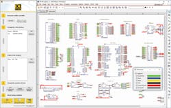
At Apex Expo, XJTAG will exhibit its new XJTAG DFT Assistant for OrCAD Capture software plug-in (Figure 3), which allows design engineers to identify and correct potential JTAG testability problems early in the design cycle, before moving to layout, saving time and cost in their overall project. Because many IC packages are inaccessible for testing using physical probes, failure to provide JTAG test access to these chips could result in a board re-spin and an expensive project.
Courtesy of XJTAG
Implementing a JTAG chain in your PCB requires compliance with DFT best practices. “Making full use of JTAG, the powerful technology available in most modern, highly functional ICs such as microprocessors, microcontrollers, DSPs, and FPGAs relies on all JTAG chains being connected correctly and properly terminated,” the XJTAG spokesperson said. “Seeing how much of your PCB can be accessed using boundary scan is also beneficial because it provides engineers with the information they need in order to design for maximum test coverage.”
The XJTAG DFT Assistant helps automate this process, without requiring the engineer to understand how boundary scan works. In a few steps, the plug-in walks the user through a fully assisted board setup and then carries out a JTAG DFT analysis directly on the schematic. The XJTAG software is making use of the JTAG standard built into many ICs, such as FPGAs, CPLDs and most CPUs. BSDL files for JTAG devices are available from IC vendors.
According to its website, Cadence OrCAD Capture helps engineers manage their PCB designs efficiently from initial schematic entry through design analysis and rule checking, layout optimization, component selection, and BOM management. Tools such as automated wiring accelerate laborious processes, viewers with color coding help inspect nets and navigate connection hierarchies, and database and search tools help streamline component selection.
“We saw that our customers could benefit from direct integration of JTAG in OrCAD Capture,” commented Kishore Karnane, director, product management, Cadence OrCAD Solutions. “XJTAG was the ideal partner to help us achieve this, bringing their specialist knowledge and their expertise in testability issues and design.”1
“We need to determine early in the design phase how to maximize test coverage using the minimum number of test points,” added Urs Allemann, director, design services, ed electronic design ag. “So it is vital to know what JTAG access is available at the schematic stage. The XJTAG DFT Assistant for OrCAD Capture makes it easy for us to see the test coverage as the design evolves, and this allows us to optimize our testing before the PCB is produced.”1
The XJTAG spokesperson said DFT Assistant also is available for Altium Designer. In related news, JTAG Technologies, also slated to exhibit at Apex Expo, recently introduced JTAG Maps, a simple extension to the Altium Designer tool suite that allows engineers to assess the capabilities of the JTAG/boundary-scan resources on their design before committing to layout.
Bare-board test
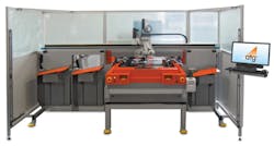
Peter Brandt, director, sales, Europe and Japan, said Xcerra’s atg Luther & Maelzer division will exhibit its A8a high-speed flying probe system (Figure 4) with eight probes for bare boards at Apex Expo. “Due to the unique multihead technology, the system reaches an outstanding performance of speed and throughput in the bare-board industry,” he said. “The test system combines the flexibility of flying probe testers with high throughput. It achieves a significant cost advantage compared to fixture testers for small and medium batches while fully meeting the requirements of the electrical test of HDI products, server boards, and back panels. The combination of automation with high throughput test systems is perfect to extend the usage of flying-probe testers to mid-size production/sample volumes.”
Courtesy of Xcerra’s atg Luther & Maelzer division
atg’s flying probe systems use direct (ohmic) and indirect (capacitance, inductance) measurement techniques and offer options for using both in combination to achieve the best reliability/performance ratio. In addition, a range of measurement methods like the trademarked Micro-Short Detection, four-wire Kelvin test, embedded component test, and LaTest (Latent Defect Test) is available to cater to specific application requirements. atg Luther & Maelzer offers fixture based Grid test systems as well as flying-probe-based test systems.
PCB repair
Also exhibiting at Apex Expo, Orbotech said it would highlight the Precise 800 Automated Optical Shaping (AOS) system, which the company said is the first solution for advanced high-density interconnect and complex multilayer PCB manufacturing that is capable of both removing (or ablating) excess copper (to repair shorts) and depositing missing copper (to repair opens). This one-stop 3D shaping solution increases PCB yield by virtually eliminating scrap, thus allowing PCB manufacturers to increase cost savings, lower their overall cost of ownership, and achieve a faster ROI, a spokesperson for the company said.
The Precise 800 employs digital additive manufacturing, representing a breakthrough in electronics micro-manufacturing production processes, the spokesperson said. The system is based on an additive technology that was developed by Orbotech over a number of years.
“PCB manufacturers are under continual pressure to produce cost-sensitive, ever-smaller, functionality-rich devices in high volumes,” the spokesperson said. “The Precise 800 meets those requirements by providing high-quality, meticulous shaping of PCBs that might otherwise have been scrapped.”
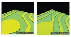
The Precise 800’s capability to automate the PCB shaping process is enabled by two new Orbotech trademarked proprietary technologies—3D Shaping (3DS) Technology and Closed Loop Shaping (CLS) Technology. 3DS is based on a series of processes, including 3D defect analysis, 3D laser shaping, and 3D visualization. By comparing the shape of the defect to real-time CAM data and simultaneously conducting 3D analysis, 3DS automatically identifies where copper needs to be added. It then guides the system’s laser to Orbotech’s Precise Stick, a high-quality metal carrier, for precise copper deposition (Figure 5). The results—which must meet strict manufacturing specifications for electrical characteristics, durability, and visual properties—can be confirmed immediately with 3D visualization.
Courtesy of Orbotech (All Rights Reserved)
CLS leverages specialized image analysis algorithms to make real-time comparisons between the actual image and the design data to detect the precise location of the shorts. It then intelligently guides the system’s laser to ablate excess copper with high accuracy.
On the horizon
Many other companies are slated to present test and inspection products at Apex Expo. Acculogic, for example, will likely highlight its line of boundary scan test tools—including the ScanNavigator integrated boundary scan test environment—which can be used throughout the product life cycle from design verification and validation and continuing into pilot production and manufacturing and onto field service and repair.
Seica, which has just turned 30, is likely to highlight its Pilot4D V8 HF, a flying-probe tester able to perform frequency measurements up to 1.5 GHz. On the software front, Aster Technologies is likely to reprise its electronica 2016 demonstration of its twSystem board-level system viewer with National Instruments’ TestStand.
Inspection companies also will be represented. YXLON is expected to explain that Volume Graphics’ VGStudio MAX 3.0 visualization and analysis software will come with YXLON’s computed tomography systems, including the YXLON FF20 CT for inspecting small-scale electronics components. Microscan is likely to highlight the latest version of its simplified AutoVISION Machine Vision Software, introduced last September, which supports the company’s new MicroHAWK smart cameras. And Sonoscan can be expected to demonstrate the THRU-scan and multigate inspection modes it developed for its C-SAM acoustic micro-imaging systems.
Finally, Cincinnati Sub-Zero (CSZ) can be expected to highlight environmental chambers used to test ICs, circuit boards, and electronic assemblies. CSZ offers products ranging from MicroClimate benchtop temperature/humidity chambers to large reach-in and walk-in rooms. Visit the online version of this article for more on IPC Apex Expo.
Reference
- “New XJTAG DFT Assistant tool for OrCAD Capture,” Case Study, Cadence Design Systems and XJTAG.
For more info
About the Author

Rick Nelson
Contributing Editor
Rick is currently Contributing Technical Editor. He was Executive Editor for EE in 2011-2018. Previously he served on several publications, including EDN and Vision Systems Design, and has received awards for signed editorials from the American Society of Business Publication Editors. He began as a design engineer at General Electric and Litton Industries and earned a BSEE degree from Penn State.
Voice Your Opinion!
To join the conversation, and become an exclusive member of Electronic Design, create an account today!

Leaders relevant to this article:
