Light provides right insight for medical imaging
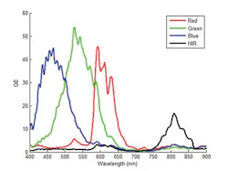
Recently, at SPIE Photonics West in San Francisco, imec introduced a new sensor with the potential to enhance developments in medical imaging. Headquartered in Leuven, Belgium, imec has its distributed R&D groups at a number of Flemish universities and globally. The new sensor includes integrated color (RGB) and narrowband near-infrared (NIR) filters (see graphic). Being able to combine these filters in one platform is something new, which the organization said has the potential to enable many different applications in medicine and beyond.
Courtesy of imec
The potential of light as a medical-imaging tool has been largely overshadowed or overlooked since Roentgen and the X-ray. Most of the high-profile imaging developments of the last century (excepting sonography) are based on slices of the electromagnetic spectrum other than the visible. But continued developments in optical science—from the observation of the spectral shift of light in passing through a substance such as water by Indian scientist C.V. Raman in the 1920s to the present—have begun to change that.
And a host of emerging technical capabilities by imec and others have enhanced the practical potential of light for medical imaging. Indeed, a recent announcement from Dublin, Ireland-based Research and Markets highlighted findings in its Global Optical Imaging Market 2017-2021. Among the firm’s observations is the fact that the market penetration of digital technologies in the optical-imaging and medical-imaging areas has become a potent driver of market growth. Furthermore, the report notes that “radiation-free” optical technology already is being used for dental diagnosis and treatment.
Julien Pincet, imec R&D engineer, said his organization’s goal was to combine the benefits of snapshot and line-scan imaging to produce an easy, fast, and usable camera system with high spatial and spectral resolution and with image formation achievable near the single-second range. “We are actually able to do that in two or three seconds,” he said. “It is not quite real-time imaging, but it is as close as we can get with current technology,” he added.
Light technology has enabled this. Hyperspectral imaging has been available for some time but it has involved bulky, heavy, and costly equipment that is really only appropriate for satellites and space agencies. “Now, with CMOS-based hyperspectral imaging, this opens up more affordable technology that can be scaled to serve many new fields,” he said.
imec’s RGB-NIR bandpass filter and design-pattern implementation can be tuned to match requirements of a specific application case such as the wavelength of a particular laser or LED light, he noted.
Leveraging its own background in CMOS scaling as well as its semiconductor fab, equipment, and process technology, imec also designs and manufactures interference-based optical filters at wafer level, deposited and patterned directly on top of the CMOS image sensor pixels. It’s “an affordable, high-resolution, and high-speed solution,” explained Andy Lambrechts, program manager for imec’s integrated imaging activities, in a press statement. “This capability to integrate a color view with one or several NIR narrowbands will be a key enabler for next-generation 3D and imaging development,” he added.
Yet another recent announcement underscores the quality of new developments in the field. Leti and PYXALIS, a company based in Moirans, France, specializing in high-performance image sensors, announced a new technology, cleverly named Owly-eyed, that lowers readout noise for image sensors down to a 0.5 electron noise value and improves low-light image sensing capabilities. Owly-eyed is based on a patented electrical architecture of the pixel readout that can be integrated in image sensors, according to the organizations, to meet growing demand for more sensitive CMOS image sensors. It has been adapted for PYXALIS, which will offer it in its next-generation image sensors, the companies said.
In the Owly-eyed technology demonstrator, a sub-0.5 e−rms temporal read noise has been achieved on a VGA format CMOS image sensor implemented in a standard CMOS process. The low-noise performance is achieved exclusively through circuit optimization without any process refinements.
“In this common lab with PYXALIS, we’ve developed a low-noise image technology that provides state-of-the-art advanced imaging for next-generation applications in a wide range of markets and industries,” said Marie Semeria, Leti’s CEO, in a press statement. “This CMOS-based device, which can be adapted for multiple uses, is another strong example of how Leti’s broad technology innovations make our partners more competitive in their industries,” she said.
“Leti’s Owly-eyed technology is a major improvement in low-noise imaging,” said PYXALIS CEO Philippe Rommeveaux. “Combined with our capacity to offer advanced sensors with high digital integration and high dynamic range, it will allow us to establish a new performance standard,” not only in medical or biomedical areas, but also in low-light applications in the surveillance, science, defense, and aerospace markets.
About the Author

Alan Earls
Contributing Editor
Voice Your Opinion!
To join the conversation, and become an exclusive member of Electronic Design, create an account today!

Leaders relevant to this article:

