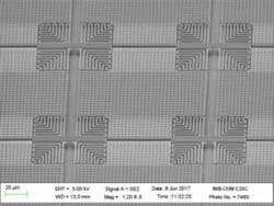
Nanusens addresses stiction in CMOS NEMS inertial sensors
Barcelona, Spain. Nanusens has announced that its CMOS nano-sensor technology has been successfully used to solve the problem of stiction in MEMS inertial sensors, which is a major source of failure for this type of sensor.
“Our first silicon nano-sensor samples from GLOBALFOUNDRIES exceeded our expectations showing outstanding resilience to stiction, with the devices going through more than 10,000 switching cycles, each equivalent to more than 1,000g shocks,” explained Nanusens CEO Dr. Josep Montanyà i Silvestre. “And the sensitivity is an order of magnitude above what is needed for a motion sensor in most applications.”
The problem of stiction in MEMS is caused by attractive forces that occur on microscopic levels such as Van der Waals and Casimir. These are surface-area dependent and not mass dependent. In an inertial sensor design, there is a proof mass connected to a spring. This mass moves when there is an acceleration, the movement is detected by the mass acting as one electrode, and the change in capacitance is measured relative to a second fixed electrode. However, if there is a large movement such as from a shock or collision, the mass goes beyond the normal range of traveling and touches a surface enclosing the sensor where it “sticks” due to the attractive forces and stops working. This can be countered by having stronger springs, but this reduces the sensitivity of the sensor. A solution to increase the sensitivity could be to increase the mass, but this results in a greater surface area for the mass and so, unfortunately, more attractive forces.
The approach used by Nanusens is to reduce the sensor design by an order of magnitude from MEMS, with linear feature sizes of 1 to 2 μm, to nano-electromechanical systems (NEMS), where the features are 0.3 μm. This feature-size reduction also reduces the attractive forces significantly as the surface-area reduction is in two dimensions—that is, almost two orders of magnitude reduction. Reducing the proof mass could result in decreased sensitivity except this is offset by reducing the gap between it and the fixed electrode. The size reduction also means that the energy stored on the proof mass when it hits the surface in case of a shock is much less, and the travelling gap is also small.
“Therefore, by reducing all the dimensions of the device, we keep the sensitivity and we increase the reliability,” added Dr. Montanyà. “In fact, we have such a gain in reliability, that we can increase sensitivity and still have a very reliable device.”
The new nano-sensors are made using standard CMOS processes and mask techniques. The inter-metal dielectric (IMD) is etched away through the pad openings in the passivation layer using vapor HF (vHF) to create the nano-sensor structures. The holes are then sealed, and the chip packaged as necessary. As only standard CMOS processes are used, and the sensors can be directly integrated with active circuitry as required, the sensors can potentially have high yields similar to CMOS devices.
Nanusens has perfected this CMOS nano-sensor technology over the past year based on developments that the key staff had completed when working at Baolab Microsystems, which closed in 2014. It was the success of this previous work that has enabled Nanusens to partner with GLOBALFOUNDRIES.
Rajesh Nair, vice president of product management at GLOBALFOUNDRIES, commented, “We have built a strong relationship with Nanusens, and we look forward to advance this new generation of sensor designs using our standard 0.18-μm processes.”
Dr. Montanyà concluded, “Nanusens decided to partner with GLOBALFOUNDRIES to develop its nano-sensors due to the outstanding technical expertise and quality of service received from their teams, together with such a large variety of CMOS nodes where we plan to move some of the devices in the future including many RF options. In addition to this, producing our nano-sensors at GLOBALFOUNDRIES, with their huge volume capacities that keep growing due to their continuous investment in their global footprint, ensures that Nanusens will have all the required production capacity that it will need in the future, and that there will never be a shortage in supplying our products to the customers. This large volume capacity is key to serve the consumer market, where demand can fluctuate very quickly, and there can be unexpected peaks.”
About the Author
RN (editor)
Voice Your Opinion!
To join the conversation, and become an exclusive member of Electronic Design, create an account today!

Leaders relevant to this article:


