New system, software, and materials augment 3D printing
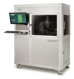
The world of 3D printing is seeing innovations regarding hardware, software, and materials as 2017 draws to a close. First, Nano Dimension in September announced the commercial availability of the DragonFly 2020 Pro 3D printer, which, the company said, can remove many of the complexities and bottlenecks inherent in multilayer PCB prototyping. The DragonFly 2020 Pro (Figure 1) replaces the desktop-sized model that was tested during Nano Dimension’s beta period and demonstrated at IPC Apex Expo 2017.1
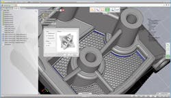
Courtesy of CoreTechnologie
“Agility and keeping pace with rapidly changing customer expectations is a competitive differentiator,” said Simon Fried, cofounder and chief business officer of Nano Dimension, in a press release. “3D printing with this next-generation Drag-onFly is transformational for electronics development. Optimizing workflows shrinks PCB design and test cycles from months or weeks to days. More and easier iterations lead to greater innovation and better business outcomes.”
The DragonFly 2020 Pro 3D printer can print high-resolution traces with its precise inkjet deposition system, and it can construct multilayer PCB features including interconnections such as buried vias and plated-through holes as well as antennas. In addition, it allows companies to keep sensitive and proprietary design information in-house during the development process.
Additive-manufacturing software
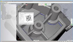
As for software, CoreTechnologie presented its new 3D_Additive manufacturing software at the Formnext trade fair in November in Frankfurt. With the tool, CAD data for 3D printing processes can be processed and analyzed with test profiles regarding different rapid manufacturing procedures.
For metal printing processes, the new software can create support structures for production as well as lattice geometries for lightweight construction and material savings (Figure 2). A graphic interface allows a direct and easy modification of critical geometry areas as well as the reduction of the complexity of the parts to be printed. The software has interfaces for tools and formats including CATIA, NX, SolidWorks, Creo, JT, and STEP.
Courtesy of Nano Dimension
CoreTechnologie also said it is addressing virtual reality and augmented reality as well as additive manufacturing with version 4.1 of its 3D_Evolution CAX data-conversion software. Version 4.1 can generate, in seconds, an envelope geometry from detailed CAD models, reducing and storing the results in accordance with VR and AR standards. The number of polygons can be decimated by 90% and more, the company said, so that large models can now be displayed quickly in augmented-reality glasses. For additive manufacturing, the software will be updated in accordance with the new 3MF and AMF formats, the company said, adding that it is working on the next major release of its tools for the next-generation of additive-manufacturing software.
Inks and alloys
As for printing inks, Nano Dimension announced in October the opening of its 8,600-square-foot nanoparticle ink production facility in Ness Ziona, Israel, where scientists will produce advanced nanoparticle conductive and dielectric inks for the DragonFly 2020 Pro. “We have made significant progress over the past several months to design and engineer an innovative continuous manufacturing process to enable us to increase production of our nanoparticle inks and compatible dielectric materials,” said Amit Dror, CEO of Nano Dimension. The process implemented at the ink production facility, located in same building as the company’s headquarters and R&D laboratories, will allow the company to scale-up and maintain its ability to supply customers with advanced materials while protecting trade secrets, he said.
And finally, Empa, the Swiss Federal Laboratories for Materials Science and Technology, contends that new designer alloys for aerospace applications can be manufactured using a 3D laser melting process. While working as an Empa researcher, Christoph Kenel completed his Ph.D. thesis describing the development of a titanium aluminide (TiAl) alloy for use in beam-based additive- manufacturing technologies. The alloy includes nanosized oxide dispersoids to improve its high-temperature mechanical properties. For his work, Empa on Nov. 13 awarded Kenel, who now works at Northwestern University in Chicago, the Empa Research Award 2017.2
References
- Nelson, Rick, “Nano Dimension highlights 3D PCB printing at Apex Expo,” EE-Evaluation Engineering Online, Feb. 19, 2017.
- Klose, Rainer, “Alloys from the laser printer,” Empa, Nov. 14, 2017.
For more information:
About the Author

Rick Nelson
Contributing Editor
Rick is currently Contributing Technical Editor. He was Executive Editor for EE in 2011-2018. Previously he served on several publications, including EDN and Vision Systems Design, and has received awards for signed editorials from the American Society of Business Publication Editors. He began as a design engineer at General Electric and Litton Industries and earned a BSEE degree from Penn State.
Comment About the Article
To join the conversation, and become an exclusive member of Electronic Design, create an account today!

Leaders relevant to this article: