Test strategy analysis has become increasingly important for finding ways to reduce test costs for system-on-a-chip (SoC) semiconductor devices. Every SoC device’s test flow is unique and requires a thorough analysis to determine the best strategies to use for reducing the cost of test (CoT). The test flow always includes a wafer-sort insertion and for packaged devices, final test insertions. Typical test flows may include two to five or more test insertions, depending on the device and end -customer’s requirements. In the past, the strategy of increasing site count at each test insertion in the flow has been a standard approach to reduce test costs.
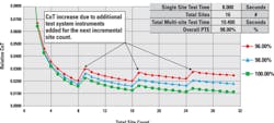
As site count is increased, the CoT typically decreases because the capital cost of the test cell is amortized over more devices being tested in parallel, which more fully utilizes the resources in the tester. When the site count reaches the point of consuming the resources in the tester, additional instrumentation is required for the next incremental site count step. This will cause an increase in the CoT for the next site count, but as the additional instrument channels are consumed by additional sites, the CoT continues to improve.
However, there is a point where the CoT curve stops declining and can inflect and begin to increase as the site count continues to increase. This is primarily driven by the parallel test efficiency (PTE) of the test solution. PTE effectively measures the degree of true parallelism of test that is accomplished and is driven by the efficiency of the test system hardware, software, and device test requirements.
Parallel test efficiency is calculated as follows:
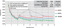
As shown in Figure 1, the cost of test improves as site count is increased until the additional incremental hardware needs to be added to the tester to accommodate the next incremental site count. The 96% PTE curve (red) shows an increase in CoT as site count increases beyond 16 sites due to the lower efficiency. This example uses a single-site test time of 8 s.
The strategy of increasing site count has other limitations that can occur before PTE is an issue. There are limitations being encountered by semiconductor manufacturers in the ability to design and fabricate the complex device interface boards (DIB) required to interface the semiconductor devices being tested to the test system.
The complexity is primarily driven by the number of signals that need to be routed from the tester channels to the multiple device sites and the additional test electronics that need to be located around each device site to perform the required tests. For wafer-sort applications, the number of pins on the probe card necessary to support all of the device test sites, the number of board layers, etc., can cause probe-card costs to increase to prohibitive levels.
Wafer sort
At wafer sort, there is a limiter to increasing site count that can be encountered before probe-card costs become prohibitive. Touchdown efficiency (TDE) is a key measure that impacts the CoT at wafer sort. TDE is a measure of percentage of die touched by the probe array on the probe card for all touchdowns on the wafer.
For example, if the probe array supports testing eight device sites and the pattern of the sites for the probes is a 2×4 array, then when a touchdown makes contact with eight die on the wafer, the TDE is 100%. If the probe array makes a touchdown at the edge of the wafer and touches fewer than eight die because some of the array is “off” the edge of the wafer, then the efficiency is less than 100%. If five of eight die are touched, then the TDE is 62.5% for the touchdown.
The following equation will determine the overall touchdown efficiency for testing a wafer:
In many wafer-sort applications, it is not desirable to have the probe array touchdown at the edge of the wafer such that some of the probes are on the wafer and some go off the edge of the wafer. This is referred to as off-wafer touchdowns. When probes touch the edge of the wafer or the surface of the wafer with no die pads, they can be worn over time if making contact with a metal layer or require more frequent cleaning when touching a passive layer.
Also, when touching off-wafer in high-temperature insertions, the probes that do not make contact with the wafer can cool and therefore will not be at the proper temperature for the next touchdown.
When off-wafer touchdowns are prevented by controlling the touchdown sequence, it is common for some die to have a second touchdown, and this needs to be considered. The calculation of TDE for this is the same as the off-wafer calculation.
The value for TDE is driven by the geometry of the wafer, geometry of the probe array, and the number of sites tested. If touching off-wafer is not desired, then it is possible that maximum attainable yield will be impacted because the probe-array geometry may prevent some die from being touched, and this is not desirable. Probe-array geometries and site count need to be readjusted to eliminate this issue as well as optimize the TDE to minimize the CoT for the test insertion.
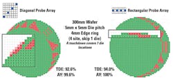
Figure 2 shows an example of not stepping off-wafer, demonstrating how a change in probe geometry can impact TDE and attainable yield (AY) for testing four sites. It also shows where die cannot be touched due to the length of the diagonal on the wafer and the length of the probe array being larger (pink Xs on the left side). This condition should always be avoided to ensure AY is 100%.
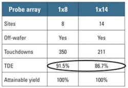
In the example of Table 1, if TDE was not considered, the CoT for 14 sites was calculated to be 2% better than for eight sites. When TDE is included in the same CoT calculation, the 8-site configuration has a 5.1% better CoT than 14 sites.
Final test
Final (package) test is typically a higher-cost test insertion. The higher cost is driven by the handler cost, limited site count, lower utilization rate, and higher cost of yield loss. A common CoT-reduction strategy is to reduce the total number of test insertions across the test flow with particular focus on final-test insertions. However, there are some situations where this may not reduce the CoT but have the opposite effect of increasing the CoT.
For example, if an SoC device requires a set of analog tests requiring 25% of the test execution time and the remaining digital tests are 75% of the test execution time, then during 75% of the testing, the analog instruments are idle. Also, if the analog tests have a higher failure rate than the digital tests, then it may be best to perform two separate test insertions.
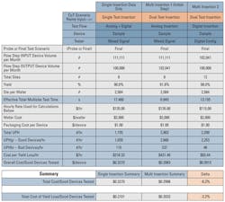
The first test insertion would perform the analog tests followed by the second insertion performing the digital tests. There are several variables that need to be considered before making a conclusion on single- versus dual-insertion steps, including the test time division between the two strategies, site count and PTE of each insertion, cost of two separate device interface boards (DIBs), test-cell cost, and yield of each insertion (at dual) versus a single insertion. Comprehensive CoT calculators should be available from your test-equipment provider to assist with these calculations.
Yield at each test insertion is a critical parameter to consider when analyzing the total test-flow cost. The total cost of yield loss (CoYL) includes the cost of yield loss at each test insertion. The insertion CoYL is determined by the cost of the die, cost of each previous test insertion, cost of the current test insertion, and the cost of the package and assembly if at final test. The total CoYL is then amortized and added to the cost of good devices tested to determine the complete test-flow cost.
In general, test strategies that perform low yielding tests as early in the test flow as possible will minimize the impact of yield on cost. In many situations, data needs to be taken from multiple device lots to determine how to shift tests between different test insertions (including wafer test versus final package test) to execute low yielding tests as early in the flow as possible.
Table 2 shows that under some circumstances, dual-insertion tests may have a lower CoT than a single insertion. In this example, the analog tests have a lower yield than the digital tests, and with a shorter test time, bad devices are quickly removed from the test flow. The dual-insertion scenario results in an 8% reduced CoT vs. a single insertion.
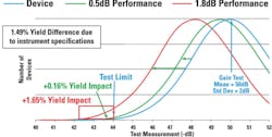
The test system instrument performance also plays a key role in the CoYL. An example of a device transmitter gain measurement with a customer specification of -50-dB transmit level can be used to describe the impact. If the average device performs at -50 dB and has a standard deviation of 2 dB, then a high test limit of -44 dB and a low test limit of -56 dB would be set as the ±3 sigma test limits.
If the test system instrument has a specification of ±0.5-dB accuracy when measuring a signal at this level, then there could be a 0.16% impact on device yield if the measurement is at the +0.5-dB performance level. If the test system instrument has a specification of ±1.8 dB accuracy then there could be a 1.65% impact on device yield. The difference of 1.49% yield will translate into a significant cost of test difference (Figure 3).
And as previously discussed, if this test is performed at a final test insertion, then the cost impact of the yield loss will be much higher than if this test is performed only at wafer sort.
Conclusion
Increasing site count for many SoC devices is becoming more and more challenging to implement. In general, the future trend for SoC device site counts is to either remain at the current level or make an additional step. Therefore, additional test strategies need to be explored in order to continue to reduce the CoT. This is becoming even more important because test times are tending to increase in many device areas due to higher transistor counts, more analog functions, and reductions in acceptable levels of defect parts per million (DPPM) by automotive manufacturers for safety as well as consumers for their electronic devices.
Standard “rules” or “practices” cannot be generally applied to reducing test costs across the total test flow of a semiconductor SoC device. Every test flow is unique, and semiconductor manufacturers need to analyze each flow to identify additional strategies to continue to reduce the overall cost of test for shipping good devices to their customers.
About the author
Randy Kramer is the director of SOC Factory Applications Engineering for Teradyne Inc. located in North Reading, MA. He has been with Teradyne for 35 years working in various applications engineering and marketing roles. He graduated from Rensselaer Polytechnic Institute in 1982 with a BSEE degree.
About the Author

Randy Kramer
Voice Your Opinion!
To join the conversation, and become an exclusive member of Electronic Design, create an account today!

Leaders relevant to this article:
