Tools from software to X-ray systems round out PCB test and inspection
Printed-circuit-board quality challenges extend from design through production test and inspection and on to field diagnostics. Meny Gantz, VP of marketing for Orbotech’s PCB division, cited some key trends in the PCB arena. The increasing sophistication of smartphones, the proliferation of automotive electronics, the emergence of Industry 4.0, and the rollout of 5G are all leading to small-form-factor, high-density-interconnect (HDI) boards requiring fine traces with good impedance control, which in turn requires tighter control of conductor dimensions, he said.
Keysight Technologies product manager Ban-Kwan Wong also cited Industry 4.0, noting that everyone is talking about how it will transform manufacturing. A key component of Industry 4.0, Wong said, is data analytics, which can help businesses improve their operations and reduce downtime.
Ryan Jones, senior technical marketing engineer at Corelis, said lack of physical access continues to be the biggest challenge in circuit-board testing. And the problem is exacerbated by the trends Gantz mentioned.
Applying JTAG/boundary scan
Simon Payne, CEO at XJTAG, commented, “The increasing number of I/O pins on high-density multilayer circuit boards are often impossible to test with traditional methods,” and even where they can be applied, they require large, expensive equipment and fixtures. “The nonrecurring engineering (NRE) costs of building test fixtures can be prohibitively high,” Payne said. “In many cases, using JTAG/boundary scan will allow the fixture to be dramatically simplified, resulting in significant cost savings.”
Elaborating on boundary scan, Payne added, “Although JTAG has been around for over 25 years and is built into CPUs, programmable devices, and other ICs, its potential is often undervalued, leading to poor implementation during a circuit board’s design, stopping it from reaching its full test potential.”
Jones at Corelis commented, “Applications in JTAG have evolved tremendously over the years.” He finds surprising the continuing misconception that JTAG is a manufacturing-only test solution. “The reality is, JTAG is a versatile test technology that has undoubted usefulness in production and manufacturing, but nowadays there are many other applications that can help engineering departments better meet test requirements; assist in prototype bring-up, debug, and troubleshooting; reprogram devices in-circuit to speed up design validation efforts, and play an ever more important role in the overall design-for-testability of a product,” he said.
JTAG can help meet challenges on several fronts. “While JTAG by definition provides test access where there is none, it is not universally available on every possible pin,” Jones said. “We do offer external modules to add JTAG test capability, but this is only useful if access is available.” With regard to high-speed signals, he said, “We provide support for 1149.6 testing when devices with that technology are available. Alternatively, our embedded test suite can test high-speed circuits at-speed when a supported processor is available.”
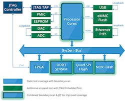
Jones also addressed programming speed. “Flash devices continue to grow in size and density,” he said. “JTAG is convenient for in-circuit programming, but the tradeoff is that it is typically slow due to limitations in TCK rates and scan-chain length. Our software automatically optimizes devices for minimal scan-chain length, and our hardware is able to compensate for delays in JTAG scans to maximize clock rates.” Alternatively, a target-assisted method can utilize an on-board JTAG-compatible CPU to conduct flash programming operations at nominal board speed, he said. Figure 1 illustrates the test coverage that JTAG can achieve.
“ScanExpress is our flagship brand of JTAG tools covering the broad spectrum of circuit-board test,” Jones said. “We try to put out two major version updates annually, supported by point releases to address specific customer issues that arise. The ScanExpress family consists of separate, yet connected, applications covering test procedure development, design-for-test reporting, test-program sequencing and execution, fault reporting and diagnostic information, in-circuit programming, and even functional test.”
Data analytics
Keysight Technologies addresses PCBs from a variety of perspectives, and the company’s Wong elaborated on one of them. “Today, everyone is talking about Industry 4.0 and how it will transform manufacturing,” he said. A key component of Industry 4.0 is big data analytics, which he described as “…the ability to intelligently use manufacturing data to drive manufacturing KPIs (yield, quality, asset utilization, and throughput).”
He said every business relies on data to drive improvements, with 99% being historical data that focuses on descriptive and diagnostic analytics. “Descriptive talks about what happened,” Wong said. “Diagnostics talks about how and why it happened.” Keysight considers descriptive and diagnostic analytics to be level 1 and level 2 analytics, and Wong continued, “It’s important to move up the data-analytics value chain by focusing on what we call level 3 and level 4. Level 3 talks about the ability to predict failures before they happen, and Level 4 talks about prescriptive analytics; it’s about the use of emerging technologies and goes beyond descriptive and predictive models by recommending one or two more causes of action and showing the likely outcome of each decision.”
Asked about challenges customers are facing, Wong said, “All machines are prone to failures. You are looking at five unplanned downtimes a year on average, which may cost you more than $25k of productivity loss per incident. On the other hand, your customer constantly demands for quick root-cause analysis to improve their operational KPIs. Big data analytics is rapidly becoming a very important driver for operational improvements. However, it can be very daunting and time-consuming when analyzing months or years of measurement and process data just to isolate the root cause.”
Wong suggested you need an automated analytics tool that provides greater insight into your operations, with data that is actionable and in real time. “What if you can get an instant alert when an anomaly in your measurement data, metadata, machine-health data, or process data is detected?” he asked. “What if you can monitor your global operations data anywhere, anytime and get anomaly alerts via email, SMS, or mobile applications that say your ICT has a 90% probability that it will fail within the next 48 hours?”
Debuting at IPC Apex Expo
At IPC Apex Expo Feb. 27 through March 1 in San Diego, Keysight will demonstrate the ability to get answers to such questions with the launch an Industry 4.0-ready data-analytics solution called Pathwave Analytics (Figure 2). According to Wong, “Keysight’s Pathwave Analytics is an Industry 4.0-ready electronics manufacturing data-analytics solution that performs advanced analytics using manufacturing process, test, and equipment data to drive manufacturing improvements and efficiencies. Its patented advanced algorithms perform an extensive range of data analytics that unlocks deeper insights about your manufacturing process, data, and equipment….”
Wong said Pathwave Analytics transforms complex information with data visualization into reporting dashboards; performs intensive data mining, data search, and multilevel drill-down analysis; anticipates anomalies in equipment, processes, or products to mitigate risks of failures or down time; and optimizes processes through machine learning, being capable of implementing solutions without human intervention.
“Its platform-agnostic nature means that the platform can be seamlessly integrated into any existing equipment or database with minimal changes, keeping investment costs low,” Wong said, adding that the database can be configured on premises or in the cloud, giving you the flexibility to scale as your business grows.
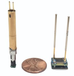
Also at Apex Expo, Keysight will unveil its nanoVTEP next-generation vectorless test solution (Figure 3). “The concept of detecting PCA open signal pins with capacitive-coupling techniques has been around for over a decade,” said Eric Chua, product manager for Keysight’s i3070 in-circuit test systems. “It is well understood and implemented by various ICT vendors in a similar form. It involves elevating an amplifier and sensor plate over the device-under-test (DUT) with a pair of hanger probes, to detect minute signal differences between a good and bad connection. As IC packages shrink and I/O pins increase, it gets increasingly challenging to mount these assemblies within limited fixture space.”
He continued, “Keysight’s solution overcomes this constraint by reducing the overall hardware footprint, driving new opportunities to improve coverage on densely populated boards.” Keysight, he said, leverages advanced manufacturing techniques and has redesigned its signal amplifier to fit into a single, small diameter barrel. “With a much smaller form factor, our solution is positioned to complement high-density probing, where conventional vectorless test products cannot be deployed due to space constraint,” he said.
JTAG for test and programming
XJTAG at Apex Expo will exhibit its boundary-scan system for testing and programming high-density printed circuits and BGA boards. “XJTAG tools are designed to be easy to learn, simple to use, and cost-effective to deploy,” Payne said. “XJTAG products reduce the cost of developing expensive test fixtures and complex test systems, giving you dual savings on NRE costs. Engineers can simplify their test systems by using boundary scan to reduce the number of probes needed in a test fixture while still maintaining or improving test coverage. Using the built-in library of test models and intuitive user interface can save test development time. Tests can be quickly generated to identify design issues in prototype designs and faults on production boards.”
He added that the XJTAG tool can test a high proportion of circuit boards including FPGAs, CPLDs, processors, DSPs, and DDR memory as well as devices with SPI and I2C interfaces. The same tool also enables in-system programming of FPGAs, CPLDs, and flash memories, reducing the number of steps and handling operations needed in the production process.
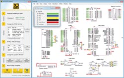
Payne also cited XJTAG DFT Assistant, which enables a circuit-board designer to check the JTAG chain implementation and the test access it affords. “Until now, PCB design tools did not include a way to check JTAG testability,” he said. “The XJTAG DFT Assistant enables PCB designers to automatically validate, at the schematic-capture stage, that components can be accessed for boundary-scan testing.” Consequently, users can “…detect and correct JTAG problems at the design stage before the PCB is produced, helping to prevent costly re-spins and project delays.”
He added that XJTAG DFT Assistant (Figure 4) is free and supports leading EDA tool vendors including Altium, Cadence, Mentor, and Zuken. “Unexpected problems can cause major delays in time to market; XJTAG DFT Assistant reduces risk by helping companies get their design right first time,” he concluded.
PCB inspection
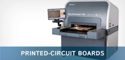
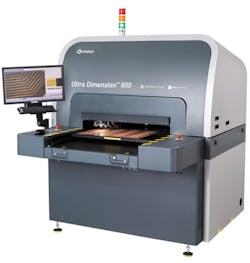
Addressing PCB inspection at Apex Expo, Orbotech will highlight its new Ultra Dimension automated optical inspection (AOI) system (Figure 5) for PCB production. Commenting that AOI by itself is not sufficient, Gantz described the Ultra Dimension as a 4-in-1 solution that integrates pattern inspection, laser via inspection, remote multi-image verification, and 2D metrology into a single system that sets new standards for the AOI-room workflow, minimizing floor space and manual handling and reducing total cost of ownership by up to 35%. The system, he said, targets premium segments involving advanced flex, HDI, and SLP/mSAP (substrate-like PCB/modified semi-additive process), giving manufacturers the flexibility to inspect a variety of applications and materials while eliminating the need to use inspection masks, which can cause defects to be overlooked.
Ultra Dimension’s combination of high precision and high-quality pattern inspection and laser via (LV) inspection in a single scan is powered by Orbotech’s proprietary Triple Vision Technology and Magic Technology. By using varied light settings and three different types of images, these technologies enable Ultra Dimension to improve detection capabilities significantly, reduce false alarms, and decrease inspection set-up time.
Orbotech’s 2D metrology automatically measures both top and bottom conductor widths for lines and pads of a wide variety of shapes, enabling the higher accuracy and impedance control necessary for SLP/mSAP as well as advanced HDI applications.
Orbotech’s Remote Multi-Image Verification (RMIV) enables the remote verification of multiple image defects, which are automatically and simultaneously acquired during the inspection process. Orbotech’s multi-image technology enables operators to accurately differentiate between real and false defects, which are then sent to offline RMIV stations. Ultra Dimension with RMIV also reduces the number of verification stations required, thereby freeing up valuable floor space in the AOI room and allowing manufacturers to significantly cut their overall labor and operational costs.
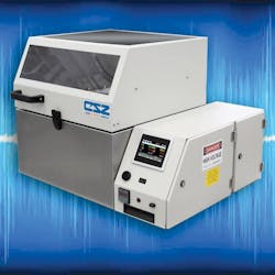
Other products to be exhibited at Apex Expo range from vibration tables to flying probers. CSZ said it would exhibit its TCB-1.3 benchtop vibration table (Figure 6), which is suitable for reliability testing of circuit boards and electronics. The dual-purpose vibration table is available in a 16” x 16” table size and may be used as a standalone vibration table or placed inside of an environmental chamber for combined vibration and temperature testing. Equipped with an all-axis vibration system, the TCB-1.3 utilizes four pneumatically-actuated vibration hammers providing 6 DOF random vibration along the x, y, z axes and roll, pitch, and yaw rotation. The chamber comes standard with two accelerometers, one for control and one vibration monitor with a vibration range of 1 to 60g RMS.
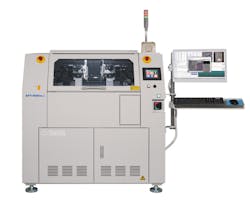
Finally, TEXMAC Inc., the exclusive authorized distributor of Takaya flying probers in North America, will highlight the new Takaya APT-1600FD advanced flying-probe test system (Figure 7). The APT-1600FD incorporates six top-side flying probes and four bottom-side flying probes.
The APT-1600FD architecture provides average head-speed increases of up to 50% with throughput improvements of 30 to 50% over existing models. The APT-1600FD incorporates a new 10-flying-Z-axis design, including four vertical flying probes that provide access to test points where conventional angled probes failed to contact. Improved “soft touch” controls virtually eliminate probe contact marks without compromising probe speed.
The system is also equipped with a laser measuring device to allow compensation for any warpage of the board under test and to accurately measure the height of any component on the board. The upgraded X/Y stage, combined with the positioning accuracy from its enhanced optical system, provides a 25% improvement in probing accuracy over previous-generation Takaya systems.
The prober’s new measurement system includes multiple 4-quadrant source and measurement units, an AC sine- and square-wave generator, and a frequency counter. An enhanced function scanner board and communications software make it easy to connect external instrumentation for additional functional-test capabilities.
Other companies haven’t disclosed their plans for Apex Expo, but recent new-product introductions suggest what they might exhibit. For example, in November, Aegis Software introduced the latest version of its manufacturing execution software (MES): FactoryLogix 2017.1. The company said FactoryLogix 2017.1 delivers advancements across the entire platform to streamline production engineering and planning, support the development of on-the-fly adaptive processes, improve shop-floor ergonomics, facilitate compliance reporting, and offer a plug-and-play connectivity backbone for the connected ecosystem.
In addition, YXLON chose productronica in Munich in November to launch its Cheetah EVO and Cougar EVO X-ray inspection systems. The company said a “one size fits all” system no longer delivers the best solution for SMT, semiconductor, and laboratory applications—consequently, it now offers systems that address the specific challenges of the different sectors.
And finally, also at productronica, Saki Corp. introduced its new 3Di AOI system, which delivers high speed (5,700 mm2/s), high accuracy, height repeatability, and scalable resolutions of 7, 12, and 18 µm for boards weighing 12 kg.
For more information:
About the Author

Rick Nelson
Contributing Editor
Rick is currently Contributing Technical Editor. He was Executive Editor for EE in 2011-2018. Previously he served on several publications, including EDN and Vision Systems Design, and has received awards for signed editorials from the American Society of Business Publication Editors. He began as a design engineer at General Electric and Litton Industries and earned a BSEE degree from Penn State.
Voice Your Opinion!
To join the conversation, and become an exclusive member of Electronic Design, create an account today!

Leaders relevant to this article:
