IEDM sees transistor, memory, laser innovations
The International Electron Devices Meeting (IEDM) held Dec. 2-6, 2017, in San Francisco offered imec and Leti an opportunity to disclose several innovations. imec announced three new developments: ultralow contact resistivity of 5×10⁻¹⁰ Ωcm2 for gallium (Ga)-doped p-germanium (Ge) source/drain contacts, multiple key process optimizations for vertically stacked gate-all-around (GAA) silicon nanowire transistors, and a power-performance-area-cost (PPAC) analysis of different sequential 3D-integration variants using advanced 5-nm and 3-nm CMOS technology nodes. Leti, a research institute of CEA Tech, demonstrated significant improvements in the field of memory systems and announced it has integrated hybrid III-V silicon lasers on 200-mm wafers using a standard CMOS process flow.
Ultralow contact resistivity
imec said its results, with regard to ultralow contact resistivity, are important in light of further downscaling of the CMOS source/drain contact area, which is challenged by a parasitic source/drain resistance that results in suboptimal transistor functioning. The low contact resistivity and high level of Ga activation were achieved after nanosecond laser activation (NLA) at low thermal budget. The results show that highly Ga-doped Ge-rich source/drain contacts provide a promising route for suppressing parasitic source/drain resistance in advanced pMOS devices.
High dopant activation is known to be an attractive approach for lowering source/drain contact resistance, imec said. Traditionally in pMOS devices, Si source/drain contacts with high boron (B) activation are used. But in more advanced pMOS devices, Ge- and SiGe(Sn)-based source/drain contacts are a promising alternative since they introduce beneficial strain. However, the higher the Ge content, the lower the boron activation and solubility in Ge or Ge-rich SiGe.
The new findings result from a comprehensive study of Ga dopant activation in Si, Si0.4Ge0.6, and Ge conducted by imec, KU Leuven (Belgium), and Fudan University (Shangai, China). In this study, either rapid thermal annealing (RTA) or Applied Materials’ Nanosecond Laser Activation (NLA) were used as dopant activation technologies, after Ga ion implantation. imec reported that the record low contact resistivity of 5×10⁻¹⁰ Ωcm2 and a high dopant activation level of 5×1020 cm-3 were obtained for Ga-doped Ge source/drain contacts after NLA. The low contact resistivity can be attributed to a beneficial Ge/Ga surface aggregation following the NLA process. With RTA activation at 400°C, a contact resistivity as low as 1.2×10⁻⁹ Ωcm2 was reported. The study shows that Ga might be preferred over B as a dopant for Ge or high-Ge content source/drain contacts in pMOS devices.
“For the first time, we have achieved contact resistivities far below 10-9 Ωcm2 for high-Ge content source/drain contacts,” said Naoto Horiguchi, distinguished member of the technical staff at imec, in a press release. “This proves that Ga doping and activation by NLA or RTA are an attractive alternative to boron doping for these source/drain contacts. It provides a possible path for further performance improvement using the current source/drain schemes in next-generation technology nodes.”
The results were obtained at low thermal budget activation, making Ga doping particularly attractive for devices that require low-thermal budget processing.
GAA MOSFETs
GAA MOSFETs based on vertically stacked horizontal nanowires or nanosheets are promising candidates to succeed FinFETs in sub-5-nm technology nodes, thus extending today’s CMOS technology beyond its scaling limits, imec said, adding that this innovative transistor architecture offers more aggressive gate-pitch scaling than FinFETs because it achieves a better electrostatic control. Moreover, in highly scaled standard cells where only one fin device is allowed, nanosheets provide more current per footprint than fins and thus can drive higher capacitive loads. Finally, integrating nanosheet devices with variable widths in a single platform enables power/performance optimization with high granularity.
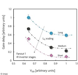
As with every disruptive innovation, this new architecture demands process optimizations, imec said. At IEDM, a team of researchers from imec and Applied Materials demonstrated multiple optimizations for the fabrication of stacked silicon nanowire and nanosheet FETs. The first process optimization is the implementation of SiN shallow trench isolation (STI) liners that suppress oxidation-induced fin deformation and improve the shape control of the nanowire or nanosheet. Second, Applied Materials’ Selectra Etch was used to enable nanowire/nanosheet release and inner spacer cavity formation with high selectivity and without causing silicon reflow. Finally, for the first time, ring oscillator circuits were reported based on stacked silicon nanowire FETs, including dual work function metal gates for threshold voltage control. Figure 1 shows ring oscillator gate delay versus VDD for stacked silicon nanowire FETs. The gate delay reduces with increasing VDD and with decreasing LG, confirming ring oscillator functionality.
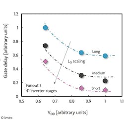
Courtesy of imec
imec also presented a study on the reliability of GAA nanowires, showing that the degradation mechanisms and their origins are similar to the one in planar devices. The modeling of the degradation including various channel hot-carrier (CHC) modes as well as positive bias temperature instability (PBTI) allows an extrapolation to 10-year lifetime in the full bias space. The obtained safe operation area (SOA) was used to optimize device operation. An extra degradation mechanism that must be taken into account is self-heating, which is important in such confined structures. Finally, in a study on ESD diodes in sub-7-nm GAA nanowire technology nodes, imec proved that the diodes’ performance is significantly impacted by some of the process options and that optimizations are needed, such as a wraparound contact (WAC) that can increase contact area in a scaled fin pitch and can be combined with GAA.
“GAA nanowire transistors are key in further CMOS scaling,” stated Horiguchi. “Earlier this year, we demonstrated standalone transistors and CMOS integration; now the next step was taken with a full demonstrator, showing the enormous promise this technology holds for realizing the sub-7-nm technology nodes.”
PPAC analysis of 3D variants
Finally at IEDM, imec presented what it called the first PPAC analysis of different sequential 3D-integration variants using advanced 5-nm and 3-nm CMOS technology nodes. The most significant benefit was found for a heterogeneous sequential-3D integration approach that uses different device layers (or tiers) for the nonscalable (analog and I/O) and scalable parts (logic and memory) of the system. These results confirm the potential of heterogeneous sequential-3D integration as a possible route for heterogeneous scaling—an emerging approach that integrates multiple transistor architectures in one system-on-chip.
Sequential-3D integration (S3D) is widely viewed as a promising alternative to continue the benefits offered by semiconductor scaling, imec said. S3D involves the vertical integration of sequentially processed device layers (or tiers) with isolation and interconnect layers in between. Three levels of granularity can be defined, depending on where the partitioning and stacking take place: at the transistor level (T-S3D), cell level (C-S3D), or IP block level, also called heterogeneous S3D (H-S3D). H-S3D is considered as a possible enabler for heterogeneous scaling. Compared with traditional through-Si-via (TSV)-based 3D-integration techniques, S3D in general offers a higher interconnect density and a more precise (lithography-defined) alignment of the stacked transistors, cells, and IP blocks.
imec said that for the first time ever, it has quantified the PPAC benefits of the various S3D variants for 5-nm and 3-nm technology nodes. To meet the challenges for S3D fabrication, the imec team used advanced technologies in some of the most critical process steps. The largest PPAC benefit was found for a heterogenous S3D use case, where the logic and memory part is scaled to iN5 technology, and the remaining nonscalable part (analog and I/O) is manufactured in N28 technology in the top tier. For this use case, despite a high wafer cost, a die cost reduction of 33% was achieved with respect to a 2D-SoC implementation with 125-mm2 die size.
“Our results demonstrate the potential of S3D technology, which benefits the implementation of next-generation application hardware such as 5G and artifical intelligence,” said Nadine Collaert, distinguished member of the technical staff at imec.
imec said its research into advanced logic scaling is performed in cooperation with imec’s key CMOS program partners, including GlobalFoundries, Huawei,
Intel, Micron, Qualcomm, Samsung, SanDisk/Western Digital, SK Hynix, Sony Semiconductor Solutions, Toshiba Memory, and TSMC.
Memory system improvements
Leti at IEDM demonstrated significant improvements in the field of memory systems, including reconfiguring SRAM into content-addressable memory (CAM), improving nonvolatile crossbar memories, and using advanced tunnel field-effect transistors (TFET). The organization also presented a high-density SRAM bitcell on Leti’s CoolCube 3D platform, which reduces the area required for memory by 30% while maintaining full device functionality. This breakthrough points the way to easing the major memory bottleneck in more complex systems on chip, Leti said, where up to 90% of the SoC area might be taken by SRAM. The breakthroughs were reported Dec. 5 at IEDM 2017 in a paper titled “Advanced Memory Solutions for Emerging Circuits and Systems.”
A key obstacle to shrinking SRAM on SoCs is bitcell-area limitations linked to required performance and yield, both of which become more challenging as technology scales, Leti said. Lowering system power consumption is also limited by memory, as the SRAM performance and its stability scale less successfully than logic performance at lower voltages. Other memories like CAM might be affected even more by voltage scaling.
“All of these obstacles become particularly important for the Internet of Things, where ultralow-power consumption and the cost of individual nodes are crucial, and SRAM limitations have a big impact on both,” said Bastien Giraud, one of the paper authors, in a press release.
Leti approached these challenges with a CoolCube SRAM design focusing on the development of a compact and functional four-transistor bitcell, along with other innovations:
reconfiguring memory between the CAM and SRAM, depending on the application;
optimizing memory using TFET, focusing on the exploitation of its negative differential-resistance effect to build ultralow-power SRAM, flip-flops, and refresh-free DRAM; and
a new compensation technique for crosspoint memory that reduces the voltage drop and leads to larger memory arrays.
Leti said its proposed CAM/SRAM outperforms state-of-the-art memories, with operations at 1.56 GHz and 0.13-fJ/bit energy per search. In addition, the proposed TFET designs are competitive in terms of area, performance, and static power consumption. Leti’s proposed compensation technique in crosspoint memory also enables the design of cost-efficient large memory arrays, while reducing the impact of temporal and spatial variations.
Short-term applications include crossbar circuits for storage-class memory and flexible SOCs with SRAM/CAM reconfigurability. “In the longer term, Leti’s CoolCube technology will be able to deliver very high-density SRAM,” Giraud said. “Enabling TFET-based DRAM and integrating TFET standard cells into CMOS designs will allow circuit designers to take advantage of the best features of both technologies.”
Hybrid III-V silicon lasers
Leti also reported at IEDM that it has integrated hybrid III-V silicon lasers on 200-mm wafers using a standard CMOS process flow. This breakthrough shows the way to transitioning away from 100-mm wafers and a process based on bulk III-V technology that requires contacts with noble metals and lift-off-based patterning.
The project, carried out in the framework of the IRT Nanoelec program, which is headed by Leti, demonstrated that the hybrid device’s performance is comparable to the reference device fabricated with the current process on 100-mm wafers. The fabrication flow is fully planar and compatible with large-scale integration on silicon-photonic circuits. The results were reported Dec. 5 at IEDM 2017 in a paper titled “Hybrid III-V/Si DFB Laser Integration on a 200-mm Fully CMOS-compatible Silicon Photonics Platform.”
CMOS compatibility with silicon photonics lowers fabrication costs and provides access to mature and large-scale facilities, which enables packaging compatibility with CMOS driving circuits, Leti said.
“Silicon-photonic technologies are becoming more mature, but the main limitation of these platforms is the lack of an integrated light source,” said Bertrand Szelag, a coauthor of the paper. “This project showed that a laser can be integrated on a mature silicon-photonic platform with a modular approach that does not compromise baseline process performances. We demonstrated that the entire process can be done in a standard CMOS fabrication line with conventional processes and materials, and that it is possible to integrate all the photonic building blocks at large scale.”
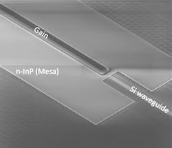
Courtesy of Leti
The integration required managing a thick silicon film, typically 500 nm thick, for the hybrid laser, and a thinner one, typically 300 nm, for the baseline silicon-photonic platform. The integration required locally thickening the silicon by adding 200 nm of amorphous silicon via a damascene process, which presents the advantage of leaving a flat surface favorable for bonding III-V silicon. The laser can be integrated on a mature silicon photonic platform with a modular approach that does not compromise the baseline process performance. Figure 2 shows a tilted scanning electron microscopy view of the III-V/Si distributed feedback (DFB) laser after the III-V patterning steps. Figure 3 shows the laser spectrum for 160-mA injection currents.
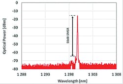
Courtesy of Leti
The novelty of the approach also included using innovative laser electrical contacts that do not contain any noble metals, such as gold. The contacts also prohibit integration lift-off-based processes. Nickel-based metallization was used with an integration technique similar to a CMOS transistor technique, in which tungsten plugs connect the device to the routing metal lines.
Next steps include integrating the laser with active silicon-photonic devices—for example, a modulator and photodiode with several interconnect metal levels in a planarized backend. Finally, III-V die bonding will replace III-V wafer bonding in order to process lasers on the entire silicon wafer.
About the Author

Rick Nelson
Contributing Editor
Rick is currently Contributing Technical Editor. He was Executive Editor for EE in 2011-2018. Previously he served on several publications, including EDN and Vision Systems Design, and has received awards for signed editorials from the American Society of Business Publication Editors. He began as a design engineer at General Electric and Litton Industries and earned a BSEE degree from Penn State.
Comment About the Article
To join the conversation, and become an exclusive member of Electronic Design, create an account today!

Leaders relevant to this article: