Nanoimprinting scales up imaging, sensing, spectroscopy applications
Nano-optics has the potential to be used for imaging, sensing, and spectroscopy, and it could help scientists improve solar cells, design better drugs, and make faster semiconductors. Nano-optic devices precisely manipulate light in ways that are unachievable by conventional optics. “Integration of complex photonic structures onto optical fiber facets enables powerful platforms with unprecedented optical functionalities,” write the authors of a paper on the topic.
A big obstacle to the technology’s commercial use, however, is its time-consuming production process. The authors continue, “Conventional nanofabrication technologies…do not permit viable integration of complex photonic devices onto optical fibers owing to their low throughput and high cost.” They offer an alternative: “In this paper we report the fabrication of a three-dimensional structure achieved by direct nanoimprint lithography on the facet of an optical fiber.” Specifically, they designed, imprinted, and optically characterized a 3D beam splitter. “Scanning electron microscopy and optical measurements confirmed the good lithographic capabilities of the proposed approach as well as the desired optical performance of the imprinted structure,” they write.1
In addition to the 3D beam splitter, the researchers have used nanoimprint lithography to fabricate a Fresnel lens on the end of an optical fiber. They note that the main advantage of the Fresnel lens compared with a conventional fiber lens is its high refractive index, which enables efficient light focusing even inside other media, such as water or an adhesive.2
The new approach—developed by scientists at the Molecular Foundry at Berkeley Lab, in partnership with users from aBeam Technologies, based in Hayward, CA—speeds the production of nano-optics from several per month to several per day. The scale-up path is to print many tips instead of sculpting individual tips. The printing approach offers speeds 30 times higher than today’s sculpting approach, researchers say, thereby opening the door to mass fabrication of nano-optical devices for widespread use.3
Recent work builds on the campanile probe, which was developed by Molecular Foundry scientists four years ago and enables spectroscopic imaging at a resolution 100 times greater than conventional spectroscopy. Fabricating campanile probes has been part science and part art, the scientists say, adding that the same applies to other nano-optical devices, such as microscopic lenses and beam splitters. These devices require milling a 3D shape with sub-100-nm scale features on the tip of a wispy fiber, which is trickier than fabricating a nanostructure on a flat surface such as a wafer.2
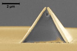
As the first step in fiber nanoimprinting, scientists create a mold with the precise dimensions of the nano-optical device they want to print. For their campanile probe, the mold of the probe’s nanoscale features includes the four sides and the light-emitting 70-nm-wide gap at the pyramid’s top. After creating the mold, the scientists fill it with a resin and then position it atop an optical fiber. Infrared light sent through the fiber enables the scientists to measure the alignment of the mold in relation to the fiber. If everything checks out, ultraviolet light sent through the fiber hardens the resin. A final metallization step coats the sides of the probe with gold layers. The result is a quickly printed—not meticulously sculpted—campanile probe. The team can make a probe every few minutes.
Figure 1 shows a pyramid-shaped campanile probe imprinted on an optical fiber captured in a scanning-electron-microscope image. The gold layer is added after imprinting. The gap at the top is 70 nm wide.
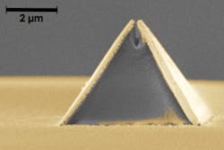
Courtesy of the Molecular Foundry, Berkeley Lab
The scientists report they have fabricated campanile near-field probes on an optical fiber using nanoimprint lithography. They describe the use of state-of-the-art ultraviolet nanoimprint lithography (UV-NIL) to fabricate functional optical transformers onto the core of an optical fiber in a single step. “Imprinted probes were fabricated using a custom-built imprinter tool with coaxial alignment capability with sub <100-nm position accuracy, followed by a metallization step,” they write.4
Their work is supported by a U.S. Department of Energy, Office of Science, Basic Energy Sciences, Small Business Technology Transfer award. A Zeiss ORION NanoFab microscope used in the research is located at the Biomolecular Nanotechnology Center/QB3-Berkeley and was funded by a National Science Foundation grant from the Major Research Instrumentation Program.
References
- Calafiore, G., et al., “Nanoimprint of a 3D structure on an optical fiber for light wavefront manipulation,” Nanotechnology, 2016.
- Koshelev, A., et al., “High refractive index Fresnel lens on a fiber fabricated by nanoimprint lithography for immersion applications,” Optics Letters, Optical Society of America, 2016.
- “Imaging Probe Printed onto Tip of Optical Fiber,” DOE Science News Source, Newswise, Oct. 30, 2017.
- Calafiore, G., et al., “Campanile near-field probes fabricated by nanoimprint lithography on the facet of an optical fiber,” Scientific Reports, 2017.
About the Author

Rick Nelson
Contributing Editor
Rick is currently Contributing Technical Editor. He was Executive Editor for EE in 2011-2018. Previously he served on several publications, including EDN and Vision Systems Design, and has received awards for signed editorials from the American Society of Business Publication Editors. He began as a design engineer at General Electric and Litton Industries and earned a BSEE degree from Penn State.
Comment About the Article
To join the conversation, and become an exclusive member of Electronic Design, create an account today!

Leaders relevant to this article: