Researchers tout imaging, lens-free microscopy applications
Hyperspectral imaging in both the visible and near-infrared (VNIR) and short-wave infrared (SWIR) wavelength ranges has been a research topic of interest for imec. Meanwhile, Leti has developed a pioneering lens-free microscope technology as well as a new curving technology for optical sensors and microdisplays. Both organizations detailed their research at SPIE Photonics West Jan. 27 to Feb. 1 in San Francisco.
VNIR is the focus of imec’s second-generation SNAPSCAN hyperspectral imaging camera, which uses an ultrasonic-speed piezo motor stage and software to acquire high-resolution hyperspectral images in less than 200 ms. imec said the technology will enable its partners to develop consistent spectral libraries and customized solutions for medical applications.
“We have been thrilled by the commercial success of the first-generation SNAPSCAN camera, which was introduced at SPIE Photonics West 2017,” said Andy Lambrechts, program manager for integrated imaging activities at imec, in a press release. “By introducing an ultrasonic-speed piezo motor stage, we can now guarantee image acquisition times of less than a second and thus minimize the effects of motion artifacts during acquisition. As a result, we can now enable many more key applications such as digital pathology, wound healing, skin diagnostics, and guided surgery.”
SWIR hyperspectral imaging imec said that semiconductor CMOS-based hyperspectral imaging filters have been integrated monolithically onto silicon-based CMOS image sensors, which have a sensitivity range from the 400- to 1,000-nm VNIR range. However, imec expects that more than half of commercial multi- and hyperspectral imaging applications—including food sorting, waste management, precision agriculture, and medical diagnostics—need discriminative spectral data in the 1,000- to 1,700-nm SWIR range.
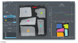
To meet this need, imec at Photonics West demonstrated its first SWIR hyperspectral imaging camera, which integrates CMOS-based spectral filters together with InGaAs-based imagers, thus combining the compact and low-cost capabilities of CMOS technology with the spectral range of InGaAs (Figure 1).
Courtesy of imec
Lens-free point-of-care system
Leti at Photonics West presented a paper titled “Lens-free Microscopy of Cerebrospinal Fluid for the Laboratory Diagnosis of Meningitis.” The technology can provide immediate results for point-of-care diagnosis, eliminating errors in counting white blood cells in cerebrospinal fluid. “Until now, this process has been operator-dependent, which limits where it can be used and increases the likelihood of errors in counting blood cells,” said Sophie NhuAn Morel, a coauthor of the paper, in a press release. “In our study, manual counts produced different results among five doctors.”
Leti’s lens-free, operator-free technology requires fewer than 10 microliters of cerebrospinal fluid to differentiate between white blood cells (leukocytes) and red blood cells (erythrocytes) in a point-of-care environment, using small equipment. “Leti’s lens-free technology can count leukocytes and erythrocytes almost in real-time and can be used in many different environments outside the lab,” Morel said.
Curving technology
And finally, Leti announced it has developed a curving technology for optical sensors and microdisplays that improves performance, enhances field of view, and compensates for aberrations in optical applications. The technology curves components such as CMOS and CCD imagers for mobile phones, cameras, telescopes, medical-imaging tools, and industrial-control equipment. Other uses include IR sensors for astronomy, defense, and drones, as well as microdisplays for automotive, augmented-reality, and virtual-reality applications.
In collaboration with LAM (Laboratoire d’Astrophysique de Marseille), Leti presented its prototype of this technology—called PIXCURVE—in the Photonics West paper “Curved Sensors for Compact High-Resolution Wide Field Designs: Prototype Demonstration and Optical Characterization.”
The demonstration is based on a 1/1.8’’-format, 1.3-million-pixel CMOS image sensor. The standard sensor structure consists of a 7.74×8.12-mm silicon die glued on a ceramic package.
About the Author

Rick Nelson
Contributing Editor
Rick is currently Contributing Technical Editor. He was Executive Editor for EE in 2011-2018. Previously he served on several publications, including EDN and Vision Systems Design, and has received awards for signed editorials from the American Society of Business Publication Editors. He began as a design engineer at General Electric and Litton Industries and earned a BSEE degree from Penn State.
Voice Your Opinion!
To join the conversation, and become an exclusive member of Electronic Design, create an account today!

Leaders relevant to this article:

