Dynamic characterization of high-speed SiC power MOSFETs and diodes
High-voltage silicon-carbide (SiC) MOSFETs and diodes combine the advantages of fast switching speeds and very low switching losses. This allows power converters designed with them to operate at higher frequencies than traditional power converters that use silicon (Si) devices. Higher operating frequencies and very low switching and conduction losses offer designers multiple opportunities for system-level optimization, including power converters with higher efficiency and power density. Reduction in magnetics size and simpler thermal management designs can also allow for total system cost reductions. In other words, although previous generations of power converters were limited by the switching speed and/or high losses of high-voltage silicon switches, SiC MOSFETs and diodes all but eliminate this constraint and provide designers with the opportunity to create super-efficient power converters that are both more compact and economical.
SiC power devices offer a variety of advantages over Si IGBTs, especially the ability to switch at higher speeds while maintaining high blocking-voltage capabilities. However, parasitic inductances due to less-than-optimal board layouts can have a major impact on SiC MOSFET and diode switching behavior. These parasitic inductances, combined with the fast dv/dt and di/dt characteristics of the SiC device, can produce problems like voltage and current overshoot, increased switching losses, and system instability. For power-converter designers to exploit the advantages that SiC devices can offer, they need tools and techniques that will allow them to study silicon-carbide device switching characteristics in depth.
On a fundamental level, traditional procedures used to characterize Si IGBTs can be applied to characterizing SiC devices. However, due to SiC’s extremely fast switching speeds, there are subtle nuances that, if not properly accounted for, can lead designers to draw incorrect conclusions. These nuances include, but are not limited to, an optimized PCB layout, adequate measurement probe bandwidth, and appropriate gate-driving strategies.
Characterizing fast-switching SiC devices
When designing power converters with slower silicon devices, characterization issues resulting from small parasitic inductances and capacitances related to the printed-circuit board layout are not so pronounced. However, when fast-switching, high-performance SiC devices are combined with less than ideal PCB design practices, additional challenges can be created, which must be addressed to make the characterization data produced useful and meaningful. These challenges include ensuring test and measurement accuracy and coping with circuit parasitics that create excessive voltage spikes, EMI, and switching losses. The highly sensitive design and integration schemes of the driving and power stages must also be considered.
Challenge #1: Ensuring test and measurement accuracy
What makes these devices more difficult to characterize? Fast switching offers lots of benefits, but it must be carefully implemented. Circuit and package parasitics and SiC’s high-speed switching capability are at the root of the issues involved. The fast dv/dt and di/dt amplify measurement inaccuracies, voltage/current ringing, etc. High dv/dt can produce large transient voltage spikes, as well as common-mode noise that can appear as damped oscillations. High di/dt generates noise that can couple with magnetic fields in the vicinity. Each of these effects can be difficult to measure and diagnose, so precise measurement tools and accurate test methodologies are essential to uncover hidden problems before they manifest themselves during the prototype stage, during product qualification, or as infant-mortality failures after the product is released.
Before power-converter designers get wrapped up in the system-level aspects of their designs, it’s critical that they have a grasp of the behavior of the power devices that will be switching high levels of power at high speeds in order to reveal potential hurdles as early as possible in the converter design process.
Measuring SiC power devices that are switching high levels of power at high speeds and obtaining accurate dynamic characterization data requires voltage and current measurement methods that can provide exceptional bandwidth and dynamic range, as well as a minimum of stray inductance and capacitance. Let’s briefly review the advantages and disadvantages of the various measurement options.
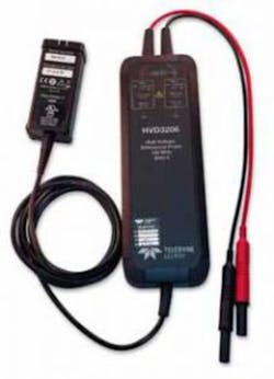
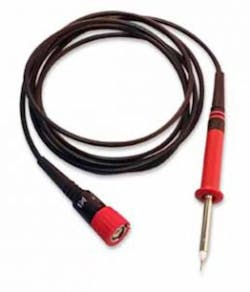
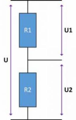
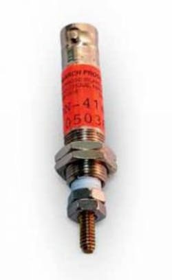
Differential probes (Figure 1) are commonly used for voltage measurements of this type; however, although they offer built-in galvanic isolation, they have relatively limited bandwidth. In contrast, the high-voltage passive probes (Figure 2) and a conventional voltage divider circuit (Figure 3) offer suitable bandwidth. However, the high-voltage passive probes require a ground-referenced measurement and lack galvanic isolation; meanwhile, a voltage divider requires that an additional resistive load be added to the circuit and also lacks galvanic isolation. All things considered, best practices would suggest using a high-voltage passive probe because its bandwidth allows it to capture high dv/dt transients.
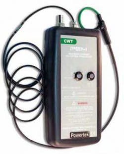
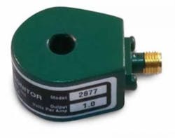
Four methods are commonly used for measuring current, but none of them are without their drawbacks. For example, a standard current probe (Figure 4) and a Rogowski coil (Figure 5) might not have adequate bandwidth to measure current ringing effects. Additionally, the Rogowski coil and the current transformer (Figure 6) aren’t capable of capturing DC information. For designs like these, which are intended only for characterization purposes where the circuit operates under pulsed conditions rather than continuous switching operation, the coaxial current shunt (Figure 7) is recommended due to its large bandwidth and high accuracy.
Challenge #2: Optimizing the power loop layout
The power electronics system can be thought of as having two main circuits: the driver loop (also known as the gate-source loop, which is discussed under Challenge #3) and the power loop (which contains the load and power semiconductor components). Because the power loop switches high levels of both voltage and current at high switching speeds, even small amounts of circuit parasitics can lead to undesirable circuit behavior that must be addressed by the designers.
Voltage spikes at switch turn-off events represent the first of these problems. The combination of di/dt and parasitic circuit inductance can cause voltage spikes, which may exceed the device’s maximum voltage rating, leading to catastrophic failure. These limitations can compromise the advantages that SiC devices can offer. If issues that lead to the voltage overshoots during turn-off events are not properly accounted for, the designer is forced to limit the speed at which the devices can be switched, select higher-voltage and more-expensive components, or resort to multilevel topologies that increase component count and complexity.
The second problem is electromagnetic interference. During switching events, ringing effects in the current waveforms create noise, which can then couple with other circuit elements. This noise essentially turns the power circuit into an antenna, broadcasting megahertz-scale frequencies. These can lead to inadvertent device turn-on and shoot-through, nearby peripheral circuit malfunctions, or failure to comply with mandated electromagnetic-compatibility regulations.
The first principle of optimizing the power-loop layout should be to emphasize board compactness and simplicity, with a focus on minimizing the overall loop area. This can reduce stray inductance dramatically, allowing designers to make the most of the high switching speed SiC power devices afford. The ideal scenario would be a loop that consists of only one point in space, that is, no trace/wire at all. A more realistic scenario is a loop with an outgoing path that overlaps with (is mirrored by, on another PCB layer) the return path, a practice known as “lamination.” In portions of the loop where lamination is not possible (such as the pins of a through-hole component), power paths should be wide enough to accommodate the current sufficiently, but minimal in length to maintain a compact overall loop.
The use of decoupling capacitors is another good practice for optimizing the power-loop layout. In the frequency domain, the process of switching at high speeds not only creates higher-order harmonics of the switching frequency (fs) but peaks related to the transient speeds that extend well into the megahertz range as well. Typically, the DC link capacitor acts as a notch filter, eliminating oscillations corresponding to fs and its harmonics of appreciable amplitude; however, it does not suppress the megahertz-scale transient-related frequencies (ftrans), which can be highly problematic for coupling into neighboring traces and circuits. To suppress peaks associated with ftrans, use relatively high-farad film capacitors connected across the DC link and placed as close to the power transistors as possible to minimize the associated loop inductance.
Challenge #3: Gate-driver design and integration
The gate drive has two main purposes: to turn power switches on and off in a stable, well-controlled manner and to incorporate intelligent power-system protection when necessary. However, accomplishing these purposes can be difficult without proper design layout and integration of the gate drive with the power stage. Common problems include unnecessary increases in switching losses, gate voltage overshoot and ringing, and EMI propagation from the power loop that leads to control-circuit malfunctions.
Even a modest level of common-source inductance (LCSI) will resist fast changes in current and increase switching losses. In the presence of high gate and source loop inductance (LG and LS), high values of di/dt can lead to overshoots in the voltage that appears at the device gate. Oscillations in the gate voltage waveform can lead to inadvertent turn-on and, as a result, potentially catastrophic shoot-through events. Hammering the device gate repeatedly with excessive voltage can also lead to device reliability and lifetime concerns.
Various methods are available to optimize the design and integration of the gate-driver circuit, but best practices start with reducing the effect of inductive coupling between the gate and power loops. Wherever possible, place these two loops in orthogonal planes. Next, just as with optimizing the power loop, work on minimizing the total gate-loop area through a combination of lamination and shortening path lengths. Finally, to reduce common-source inductance, decouple the gate loop and power loop, which can be accomplished by using packages with a dedicated Kelvin source, such as the 4-lead TO-247 or the 7-lead TO-263.
Double-pulse testing example
Double-pulse testing offers a way for power-converter designers to evaluate a SiC device’s switching performance with extreme accuracy on a per-cycle basis. This test involves turning the device on two times. The first pulse width, in conjunction with the inductor value and bus voltage, determines the current amplitude through the device during the turn-off event. During the period between the first and second pulses, the energy stored in the inductor circulates through a free-wheeling diode. This allows the same set of operating parameters to be applied to the device during the rising edge of the second pulse, the turn-on event.
Figure 8 illustrates a double-pulse test setup. In this test, an inductive load is placed in parallel with a free-wheeling diode in the upper switch position. These elements make up the free-wheeling path for current during DUT turn-off states. The DUT occupies the lower switch position. This testing configuration is useful for studying switching-energy and gate-charge characteristics of the DUT. The waveforms of interest are gate-source voltage (VGS), drain-source voltage (VDS), and drain current (ID).
The measurement equipment and the DC power supply each have their own connection to earth ground. To prevent a ground loop that may cause significant measurement errors, the test setup should be isolated galvanically from the DC power supply during testing.
In this test system, voltage-controlled relays are used for disconnecting the DC power supply (positive and negative rails) from the test setup. The DC link capacitance is sized so that it can maintain the desired bus voltage throughout the test after being disconnected from the DC power supply. This improves measurement conditions by minimizing the risk of ringing during transient events caused by ground loops. If the system can’t accommodate a big enough DC link capacitor to allow for disconnection from the DC voltage supply, the system still requires a DC link capacitance large enough to maintain DC voltage during device switching.
Measurement details
The high switching speed of SiC MOSFETs means the dv/dt and di/dt can exceed 80 V/ns and 5 A/ns respectively under certain test conditions. Because these devices are switching on and off within tens of nanoseconds, it is critical that the measurement probes have adequate bandwidth, good dynamic performance, and very small loading capacitance. As discussed in “Challenge #1: Ensuring test and measurement accuracy,” passive voltage probes are recommended for measuring VDS and VGS. A current viewing resistor (CVR) shunt is recommended for the ID measurement.
The output of the CVR should be directly connected to the oscilloscope. Probe-tip adapters should be provided on the test setup’s PCB to accommodate the following: first, a 400-MHz-bandwidth, high-voltage passive probe for the VDS measurement, and second, a 500-MHz-bandwidth, low-voltage passive probe for the VGS measurement.
Test results
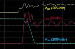
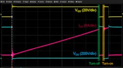
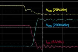
The results of a double-pulse test performed with an 800-V DC bus voltage and a device current of 20 A are illustrated in the oscilloscope screen captures of Figure 9. Figures 9b and 9c show magnified portions of the waveforms shown in Figure 9a that correspond to the turn-off (b) and turn-on (c) events. These events are used to characterize the switching behavior of the MOSFET in detail by describing its switching energy, switching speed, rise and fall times, voltage overshoot, etc.
Post-processing of test data
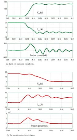
MathWorks MATLAB is a useful tool for the post-processing required to determine the numerical values for the devices’ switching characteristics. Once the raw data is imported into the post-processing environment, VDS and ID must be properly de-skewed. Figure 10 presents an example of plots generated for the turn-on and turn-off transient voltage (VDS), current (ID), and instantaneous power. Switching energy calculations and switching behavior of the DUT can be derived from these waveforms, The waveforms shown in Figure 10 indicate that, during the turn-off event, a voltage overshoot of about 70 V is present, dv/dt = 68.72 V/ns, di/dt = 1 A/ns, and turn-off loss is about 60 μJ; during the turn-on event, a current overshoot of about 10 A is present, dv/dt = 39.47 V/ns, di/dt = 5.2 A/ns, and turn-on loss is about 270 μJ. Note: switching loss values are obtained via integration of instantaneous power.
Conclusions
The double-pulse technique has proven useful for characterizing SiC MOSFET and diode switching losses, as well as other typical dynamic parameters, such as switching times, gate charge, and reverse recovery. Measuring these parameters for SiC devices requires an optimized board layout and precise voltage/current-sensing techniques. The SiC Application Support webpage and design reference files Littelfuse has developed for the Dynamic Characterization Platform (DCP) represent a good place to start.1 EE
Reference
1. “Dynamic Characterization Platform,” Application Note, Littelfuse, 2018.
About the authors
Levi Gant is a technical marketing engineer at Littelfuse Inc., headquartered in Chicago, IL. [email protected].
Xuning Zhang is the principal application engineer at Monolith Semiconductor Inc., headquartered in Round Rock, TX. [email protected].
About the Author
Voice Your Opinion!
To join the conversation, and become an exclusive member of Electronic Design, create an account today!

Leaders relevant to this article:
