Best practices for user-programmable FPGA instrumentation

Field programmable gate arrays (FPGAs) are used extensively in today’s electronic assemblies and test engineers are also choosing to incorporate user-programmable FPGA instrumentation as part of their functional test solutions. Today there are a variety of user-programmable FPGA-based instruments available to test engineers that can be used to support a wide range of applications and interfaces. These modules, which allow test engineers to create custom instrumentation and interfaces, employ a range of programming tools and architectures.
Depending on the complexity of this custom instrument, the design, integration, and supportability can prove challenging and demanding for test engineers. However, by adhering to industry standards for design tools and employing standardized FPGA interfaces, the complexity and effort required to design, deploy, and maintain these modules as part of a test system can be mitigated.
Background
FPGAs were an outgrowth of the programmable array logic (PAL) business in the late 1970s. These devices enabled design engineers to replace discrete logic chips with one programmable chip. FPGAs emerged in the 1980s as a common logic design component, with Xilinx and Altera becoming the market leaders.
Today’s FPGAs offer multiple processing cores which can run in parallel, allowing different tasks to be executed within separate “blocks” of the FPGA. Within the FPGA are a number of predefined resources which include a number of logic blocks, both configurable and fixed-function, as well as internal memory. In addition, modern FPGAs have evolved into SoC (system on chip) devices—offering higher levels of functionality including:
- Signal processing blocks
- Embedded processors
- Cache memory
- High-speed serial input/output I/O
- Graphical processing units (GPU)
- Video codecs
- Mixed-signal support
FPGA design tools & methods
Suppliers of FPGAs and FPGA modules offer tool sets that are optimized for supporting their own specific product offerings. The overall design process for an FPGA is detailed in Figure 2.
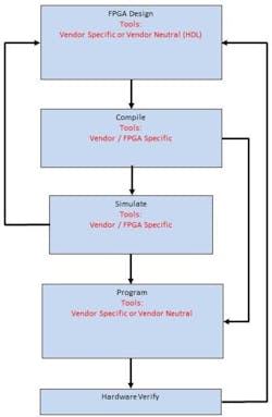
As shown in Figure 2, the FPGA design and deployment process can employ both vendor-specific and vendor-neutral tools. For the design block, the use of vendor-neutral tools, specifically HDL (either VHDL or Verilog) is highly desirable. VHDL and Verilog are open tools and are widely accepted standards. And since these are vendor-neutral tools, design portability can be maximized, minimizing vendor “lock-in” to a specific FPGA brand or module as well as mitigating dependence on one supplier/vendor. In addition, these tools are supported by IEEE standards for common HDL languages: 1076-2008—IEEE Standard VHDL Language Reference Manual and 1364-2005—IEEE Standard for Verilog Hardware Description Language.
To facilitate the design/deployment process as well as maximize supportability and life-cycle management of a user-programmable FPGA instrument, test engineers should consider adopting the following guidelines when selecting and deploying these instruments:
Use HDL where possible. HDL is supported by all major FPGA vendors’ tools and does not require any proprietary software or support. In addition, thorough documentation of HDL allows code to be ported and/or modified for use in various designs, and for support of HDL designs across organizations, functions, and time.
If design entry employs some other method (e.g., schematic or graphical), the output should be HDL, which can be read and modified.
Designers should use FPGA vendor-specific design tools (e.g., Xilinx ISE/Vivado, Altera Quartus). While not vendor-neutral, these vendor-specific tools provide comprehensive support for new and legacy FPGAs. In addition, these tools support the complete FPGA design flow from HDL entry to FPGA binary file generation.
Leveraging a standardized FPGA interface
Virtually all user-programmable FPGA modules employ external hardware or PHY interfaces that connect to the external world or UUT. These interfaces provide a range of capabilities since the FPGA itself has limited I/O capabilities (e.g., current drive, voltage levels, etc.) and is essentially a digital device with very few, if any, analog capabilities. The table below lists examples of physical interfaces that might be supported by an external FPGA interface.
| Function/Bus Interface | Physical Interface/Characteristics |
| A/D and D/A converters | High resolution and high speed converters for analog measurement/stimulus applications |
| MIL-STD 1553 | Tri-axial, transformer coupled, 18 -26 Vpp output |
| ARINC 429 | Differential, high voltage |
| RS-232 | Unbalanced, bi-polar |
| RS-422/RS-485 | Balanced, bi-polar |
| CAN Bus | Differential, CAN bus specific XCVR |
| Ethernet | Differential, transformer coupled |
| USB | Differential, logic levels |
| I2C, SPI | Buffered, logic levels |
| SpaceWire | LVDS |
| SerDes | LVDS |
| Camera Link | LVDS |
| Serial Front Panel Data Port (FPDP) | Copper/Fiber |
An alternative to vendor-specific PHY interface solutions is the VITA 57 FPGA Mezzanine Card (FMC) standard, which standardizes both the physical and electrical interfaces to FPGAs, resulting in the availability of a portfolio of off-the-shelf mezzanine boards and a standardized method for interfacing to these boards via a defined connector interface.
The FMC standard is defined by the VITA 57.1 and 57.4 specifications. Key features and characteristics of the FMC standard include:
- Defined PCB dimensions for modules that include connector location and allowance for front panel connections. FMC modules are available in single width (69 mm) and double width (139 mm) variants.
- The VITA 57.x module’s FMC connector has fixed locations for serial/parallel I/Os, clocks, JTAG signals, VCC, and GND.
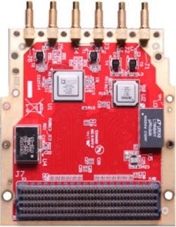
- The VITA 57.1 (FMC) modules provide access to up to 160 single-ended I/Os (80 LVDS) and/or up to 10 serial transceivers in a 40 x 10 configuration. The FMC modules can be plugged into both VITA 57.1 and VITA 57.4 compliant FPGA carrier boards. (Figure 4A)
- The VITA 57.4 (FMC+) modules provide access to up to 160 single-ended I/Os (80 LVDS) and/or up to 24 serial transceivers in a 40 x 14 configuration. Note that the FMC+ modules can only be plugged into VITA 57.4 compliant FPGA carrier boards. (Figure 4B)
With a defined high-density, high bandwidth interface, suppliers of user-programmable FPGA modules are now migrating to the FMC standard, with virtually all of the FPGA evaluation boards supplied by FPGA vendors now incorporating the FMC interface. Applications addressed by these FMC modules include:
- Analog I/O: ADCs & DACs
- High-speed digital parallel I/O: e.g., camera link, LVDS, FPDP
- High-speed serial digital I/O: e.g., fiber optics, serial front panel data port (FPDP), gigabit Ethernet, etc.
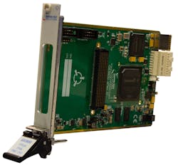
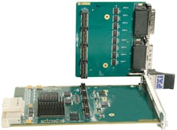
Additionally, the PXIe module depicted in Figure 5 includes full PXI/PXIe functionality:
- On-board programmable clock source for use as an FPGA timing reference or for FMC module support
- Access to the 10 MHz PXI clock and the 100 MHz PXIe clock
- Access to all PXI trigger and local bus signals
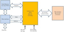
As noted above, the user FPGA’s interface to the PXIe bus is partitioned via an internal address and data bus which is accessed via predefined registers and supported by the module’s software driver and an interactive UI. The result is a simplified design/integration process since both the PXIe bus interface and associated software driver are known, tested entities. And as an added benefit, the compiled FPGA design can be loaded into on-board flash memory via this same interface, providing users with an easy way to incrementally design/test/modify their FPGA code.
Today’s test engineers can choose from a wide selection of user-programmable FPGA modules for ATE systems, with many of these modules employing proprietary design tools and methods. However, test engineers should look to adopting industry standards whenever possible when considering the use of user-programmable FPGA instrumentation. By building on established standards and standard interface modules such as VITA 57, the effort associated with the design, deployment and long-term maintenance of test systems that employ these user-programmable FPGA modules can be positively impacted.

About the Author

Comment About the Article
To join the conversation, and become an exclusive member of Electronic Design, create an account today!

Leaders relevant to this article: