Internal component features in acoustic 3D
Both X-ray and ultrasound make it possible to nondestructively examine the internal structure of solid materials. There is little correlation between their respective abilities to penetrate materials: ultrasound will pass through lead, but X-ray will not; X-ray will pass through paper, but ultrasound will not. In a great many applications, they are complementary.
Ultrasound, and particularly ultrasound at the frequencies used in acoustic microimaging, is partly reflected by all interfaces between different materials, whether the materials are solid or not. When a 100 MHz ultrasonic pulse strikes such an interface, a portion of the pulse is reflected back to the transducer that launched it and the other portion crosses the interface and moves deeper into the sample, where it may encounter another interface.
This scenario changes significantly if the pulse strikes the interface between the solid it is traveling through and a gas, typically air. Virtually all of the pulse is reflected. None travels through the gas-filled gap, even if the gap has a vertical dimension of a fraction of a micron. This high sensitivity is the reason for the widespread use of acoustic tools to image cracks, delaminations, voids, and the like.
C-mode imaging
Having struck an interface, a pulse returns in the form of an echo to the transducer that launched it. In the great majority of inspection applications, C-mode imaging is used because the user is primarily concerned with the amplitude of the echo. A pulse traveling through electronic mold compound and encountering the surface of a silicon die will be about 50 percent reflected; the other 50 percent will travel deeper. Each second the transducer scans the component, it launches thousands of pulses and receives thousands of echoes, each of which will generate a pixel in the two-dimensional acoustic image.
In grayscale C-mode imaging, areas of the mold compound that are well bonded to the die will appear medium gray, the result of the 50 percent reflection. Regions where there is a gap between the die and the mold compound will produce a bright white pixel because the reflection is virtually 100 percent.
Black pixels mean that no echo was received, and occur when a pulse encounters no interface and is entirely attenuated by traveling through a single material such as mold compound. To produce color images, a variety of maps can be used. Cracks and other gaps are often red, but the role of a particular color depends on the needs of the user.
Time difference imaging
The three-dimensional structure of features within a sample can be indicated (but not actually depicted) by an imaging mode known in Nordson SONOSCAN’S line of C-SAM tools as the Time Difference mode. Imagine a plastic IC package in which the die face is tilted rather than flat. Instead of reading the amplitude data in the return echoes, as would be done for most production-line inspection, the tool records time in nanoseconds for the echo to travel from the reflecting interface to the top surface of the sample. The time is then converted into distance, and a color map is used to correspond to the range of distances. The most distant x-y locations sending back data might be colored magenta. The nearest might be blue, with others at their assigned places along the spectrum. The percent of the pulse that is reflected is ignored in this mode, because the goal is to represent the component’s three-dimensional structure.
The result is a flat two-dimensional image that uses color to tell the viewer the relative elevation of various regions on the die face without actually depicting those differences in three dimensions.
When a pulse is launched from the transducer, the first material interface it encounters is the interface between the water that couples it to the sample and the sample itself. For Time Difference imaging, the transducer measures the time between this echo and the echo from the first internal interface.
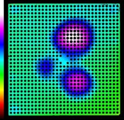
Figure 1 is the Time Difference image of the back side of an unmounted BGA device. Black items are the solder bumps. Green identifies the solder mask at the substrate level, but in three regions the surface of the solder mask is represented by colors (blue, magenta, white) that indicate a higher elevation.
The image as a whole indicates that the substrate is flat, and that the three defects, which may be voids, extend upward to various heights. The reader can envision the three-dimensional structure of the defects, but that structure is not shown directly.
In most of the 15 or so acoustic imaging modes, gates are set for the collection of returning echo signals. The gate dictates that only those echoes arriving between time A and time B (both measured in nanoseconds) will be used to make the acoustic image. In plastic packaged ICs, the echo from the top surface of the mold compound is ignored. This sample differs in that there is no gate; echoes are received from the first interface encountered at any depth.
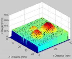
The same sample is imaged in Figure 2, but in 3D. The color map begins with green, but then runs in the opposite direction from the color map in Figure 1: the solder mask defects rise with altitude to yellow, then to red. Some of the solder bumps within the defect areas also appear taller than bumps in other regions.
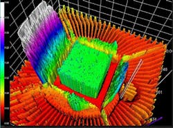
Figure 3 shows the same form of 3D acoustic imaging applied to a more complex sample—in this case, a plastic IC package that has suffered a popcorn crack that originated underneath the die and traveled upward. The IC package was scanned from above, and the results tilted to make all three dimensions visible.
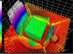
Return echoes were collected from a wide (vertically) gate, extending from just below the top surface of the part to the lead fingers. Within this gate, only the first echo arriving at each x-y location was used. If a portion of the pulse traveled deeper and generated a second echo, that second echo was ignored.
The color map used to indicate distance is at left. In the upper part of the image, there are black spaces between lead fingers because no echo was received. The surfaces of the lead fingers and the die paddle are red. At the center is the die, whose green top indicates that it lies above the lead fingers. The sides of the die are green because the vertically oriented pulses pick up no information from the sides. Software borrows the color of the die top to prevent the sides from appearing empty.
The four upward-reaching cracks surround the die. Two rise no higher than the top of the die. The crack at right rises higher; its top is blue. The crack at left rises through blue, magenta and white to the top of the color map. The top of this crack abruptly ends in a horizontal profile not because it has reached the top surface of the mold compound, but because it has reached the top of the gate just below the top surface. Echoes from above this depth will be ignored.
C-mode imaging with software stacking
There is a third way in which acoustic microimaging can produce a 3D image. First the transducer uses C-mode imaging to scan the entire thickness of the sample in multiple narrow (vertically) gates. There may be 20 or so gates. Each gate is saved as a separate image.
Software then stacks the gates, thus reproducing the entire internal structure of the component electronically. It then begins with the top gate and removes the imaging data from an area defined by the user. It does the same for subsequent gates until the desired depth is reached.
The results can be seen in Figure 4. The sample is a flip chip, imaged from the tops of the solder bumps to the substrate below. The top of the image, outside the cutout, represents the top of the underfill. The two yellow arrows point out two white voids at the top the underfill.
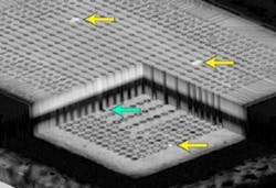
Within the planar cutout, the yellow arrow indicates a “white bump,” not connected to its pad on the substrate. The green arrow, however, points to an apparently isolated dark dot. The vertical structure behind the dot is the acoustic shadow from the solder bump, which reflected ultrasound back to the transducer and thus cast an acoustic shadow downward. Beside the solder bump at the top surface is the barely visible portion of a void. The other portion of the void, lying in the now absent cutout, likewise casts an acoustic shadow onto the substrate.
About the Author
Tom Adams
Consultant, Nordson SONOSCAN
Tom Adams is a professional science writer based in New Jersey.
Comment About the Article
To join the conversation, and become an exclusive member of Electronic Design, create an account today!

Leaders relevant to this article: