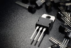
Special Report: Power Semiconductor Test
Download this article in .PDF format.
Manufacturers in the power semiconductor industry have been tackling challenges of performance, reliability, and lowering the cost of high-power devices for decades. More recently, boosting energy efficiency has taken on a higher priority. As semiconductor technology has advanced, such devices can now function with higher power, voltage, and frequency, and electronic testing vendors now must face the challenge of adapting testing needs for multiple versions of such technologies.
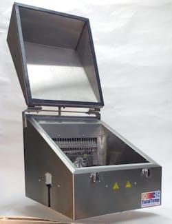
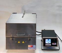
John Booher, chief technology officer at San Diego, CA-based thermal test solutions provider Total Temp Technologies, told Evaluation Engineering in late February that getting testing done in an expedient and verifiable way is another trending challenge power semiconductor test vendors are facing.
“People and companies are always looking for ways to speed the throughput, reduce costs, and make sure they get the testing done that is required without overstressing the devices,” Booher explained. “By combining conduction with convection and using a single controller that has advanced control algorithms and multiple sensing points, verifiable results can be produced quickly. Automated, coordination results of tests can be easily logged or printed to paper or PDF file if needed.”
As far as key features that customers are looking for in his company’s power semiconductor test solutions, Booher said that quality, reliability, and speed of testing are still king, while cost very often drives the features needed.
“Test equipment features that allow tests to be properly conducted in the least amount of time and for the least cost are always welcome to vendors, while less power consumption and minimizing footsteps across the lab can add up to big savings as well,” Booher said. “Good feedback from accurately performed tests points out areas where testing can be further improved, shortened or even show where not enough testing is done.”
Booher provided the following example to illustrate his point: Let’s say testing requirements say to run six cycles hot and six cycles cold, and it is discovered that more failures are occurring on the sixth cycle, this might lead to one of two thoughts, and it would be most valuable to determine which is true: 1) Is the test more stressful than it needs to be—ruining parts that might be OK in the field; or alternatively 2) A small amount of additional testing will likely weed out additional weak units. Either way, Booher explained, the result is ultimately to reduce premature thermal failures before products go into the field. Of course, catching failures before they get into the field is essentially what product testing strives for.
What’s trending?
To take a deep dive into some of the power semiconductor test trends mentioned above and beyond, we at EE asked a pool of vendors to weigh in on their observations. Here’s what they told us.
Mark Cejer, marketing director at Tektronix/Keithley Instruments: “As demand for power semiconductor devices continues to increase and as SiC and GaN are becoming more commercialized, the trend in manufacturing is toward wafer-level testing in production processes to optimize yields and improve profitability. Driven in part by a growing number of automobile and industrial applications, manufacturers increasingly need to perform breakdown testing at voltages greater than 200V. Given trends toward high-voltage wafer testing and growing volumes, the industry is moving away from the current 2-pass testing model. In this model, a wafer is first tested at 200V using a manufacturing test system. Then for high voltage validation it has to be reconnected and retested on an R&D test system that supports higher voltage. There is strong desire across the industry to move away from this productivity-killing model.”
Christian Plötz, technical sales lead at VX Instruments GmbH: “We think the number of applications—and therefore the number of needed power semiconductors—will further increase rapidly in the next years. This leads to a higher need for power components like high current semiconductor switches or whole modules like B2, B4, and especially B6-bridges.”
John Lewis, North American product manager for Rohde & Schwarz: “In power semiconductor test, the most significant trend is switching from traditional silicon technology to wideband gap semiconductors. As these devices enable higher switching frequencies, the forward-looking trend is to not only integrate passives into a semiconductor package, but also more focus on inductorless converter designs. These trends mean a broader focus on EMI compliance and debugging EMI related issues at a system level.”
Brian Walker, senior RF design engineer at Copper Mountain Technologies: “5G Semiconductors require millimeter wave measurements. Test equipment must operate at 29 GHz and higher frequencies to accommodate the new bands.”
Challenges
Many of the trends stated earlier have created new or advanced challenges for power semiconductor test solution providers. Here’s the top challenges vendors told EE they’re currently facing.
Booher, Total Temp Technologies: “Proper management of thermal stresses. Very simply, with multiple sensors, it is easy to understand the thermal profiles of various locations in the part. This allows the semiconductor test to be performed more quickly and effectively. Intelligently-designed tests performed using equipment that has easy-to-use, advanced temperature control algorithms will clearly speed the results. The ability to combine conduction and convection—plus controlling overshoot while monitoring locations that lag—will allow these substantial speed gains. Those results can easily be demonstrated from printed result profiles or log files the controller can produce. Faster test completion is plain as day.”
Cejer, Tektronix/Keithley: “Many fabs are using custom-built, hybrid test systems for high-voltage power semiconductor testing that require manually changing test setups when moving from low voltage to high voltage tests. Dual-pass testing such as this adds process steps and slows production. Most of these fabs are using GaN, which is already a more expensive material compared to silicon. As such, it is very important to them to optimize testing processes. Another challenge facing the industry is the trend toward improved measurement resolution. This is because the wide-bandgap materials have lower leakage current than silicon, often under one picoamp. This can be a challenging measurement under high voltage conditions.”
Prentice, Teradyne: “With all high-power test, controlling the residual charge and power of failing devices during test is a critical challenge. Residual charge can damage the next device under test and failing devices can cause damage to sockets and hardware. Teradyne has methodologies and specific designs in place to discharge and identify failing devices, which leads to improved device throughput as measured by units per hour.”
Walker, Copper Mountain Technologies: “High frequency measurements are more difficult to calibrate particularly due to the loss of coaxial cables. Placing the millimeter wave ‘test head’ close to the DUT minimizes this distance. We at CMT provide ‘frequency Extenders’, which operate up to 110 GHz while the interconnection RF signals to our vector network analyzer is less than 9 GHz.”
What do customers want?
We also asked vendors what are the key or newer features that their customers are looking for in power semiconductor test solutions.
Plötz, VX Instruments: “Our customers have a growing interest in short test times; higher test voltages; higher test currents; faster current rise times; low-inductive cabling and DUT contacting; isolated measurement instruments; trigger capability of all instruments; and fast instrument interfacing and command handling.”
Lewis, Rohde & Schwarz: “The reason engineers use an oscilloscope for power semiconductor testing is that they provide correlated measurements in the time and frequency domain. This correlation enables engineers to integrate their design. For example, as they make changes to the gate driver, they can see the turn-on in the time domain and its effect on electromagnetic emissions in the frequency domain. High-resolution measurements are necessary for this.”
Walker, Copper Mountain Technologies: “Test equipment must make multiple kinds of measurements to eliminate the need to switch instruments in and out of the circuit.”
Now on the market
Some of the new products/solutions that power semiconductor test vendors have recently brought to market have already been mentioned above, but let’s recap what else has been introduced as of late.
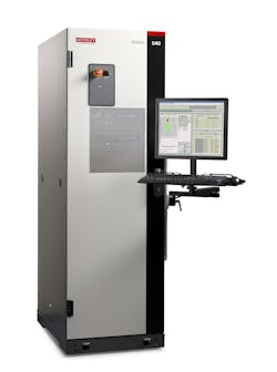
Tektronix recently introduced the Keithley S540 Power Semiconductor Test System—a fully-automated, 48-pin parametric test system for wafer-level testing of power semiconductor devices and structures up to 3kV. Optimized for use with the latest wide bandgap materials, the fully integrated S540 can perform all high voltage, low voltage, and capacitance tests in a single probe touch-down. The system can perform parametric measurements on up to 48 pins without changing cables or probe card infrastructure. It can also perform transistor capacitance measurements such as Ciss, Coss, and Crss up to 3kV without manual reconfiguration of test pins.
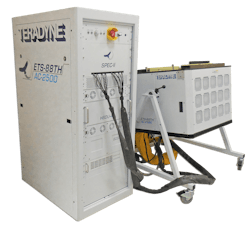
Out of Teradyne, its Eagle platform ETS-88 supports the low- to high-power discrete market, targeted at high-volume applications. The system is optimized for high throughput and low cost-of-test for single-site, multisite, and index parallel applications. The test system hardware is designed to provide independent floating resources per site to avoid resource sharing across sites while improving site-to-site isolation and measurement accuracy.
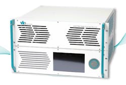
Germany-based VX Instruments has recently launched its AXC7583 and AXC7585—1.000A High Current Pulse SMUs, which are able to generate high-speed current pulses up to 1600A at 300 µs. The instruments come with a compact 19-inch form factor with only 6HE. Due to the built-in current and voltage measurement units, the pulse sources are full source and measurement units. These very short, high-current pulses reduce the demands on the DUT adaption.
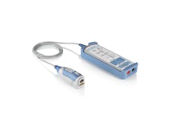
Rohde & Schwarz is now offering its RT-ZHD high voltage differential probe series, designed for complex measurements on power electronics with voltages up to 6,000V. They offer a bandwidth of up to 200 MHz, a high common mode rejection ratio—and at 0.5%, the best DC measurement accuracy available, according to the company. For lower bandwidth measurements, R&S also introduced the R&S RT-ZD002/ZD003 differential probes with maximum input voltages up to 700V and 1,400V, respectively.
Copper Mountain Technologies recently launched its CobaltFx Frequency Extension System, which allows users to build a scalable and affordable 5G testing solution, offered with four extension frequency bands up to 110 GHz. The company said CobaltFx is the first mmWave frequency extension solution that can be anchored by a 9 GHz VNA. The system has coaxial output and frequency from 18 to 54 GHz.
Market outlook
An early March report from media group The West Tribune has a more conservative outlook, forecasting a 3% CAGR for the power semiconductor market from 2018 to 2023, noting that consumer demand exceeding factory capacity and a global shortage of silicon wafer as factors expected to hinder growth.[2]
The global power semiconductor market is gaining traction, due to the incorporation of its advanced technologies in consumer electronics, such as a smartphones, smartwatches, and IoT devices, to work as small electronic gadgets and facilitate easy access of technology. Further, the enhanced features of power electronics, such as power efficiency, lightweight, high speed, and enhanced portability are the other drivers that are expected to augment the growth of the power semiconductor market, over the forecast period. Apart from technological advantages, power semiconductors are trending, due to increasing consumer interest toward electric vehicles.
Taking a more specific focus, IHS Markit reported in April of 2018 that the market for GaN and SiC power semiconductors would top $1 billion in 2020 and surge at a CAGR of 35% to more than $10 billion by 2027, energized by demand from hybrid and electric vehicles, power supplies and photovoltaic (PV) inverters.[3]
In other news and notes, on Feb. 11 of this year, JEDEC Solid State Technology Association—a global standards developer for the microelectronics industry—announced the publication of JEP173: Dynamic On-Resistance Test Method Guidelines for GaN HEMT Based Power Conversion Devices. It was the first publication developed by JEDEC’s newest main committee, JC-70 Wide Bandgap Power Electronic Conversion Semiconductors, and can be downloaded for free from the JEDEC website.
Sources
[1] “Power Semiconductor Market to Touch US$54.88 Bn by 2025 due to Rapid Adoption of Wireless Technologies – TMR”. Transparency Market Research, February 2019.
[2] “Power Semiconductor Market Share (Forecast 2018-2023) According to | Business Outlook, Top Companies, Key Regions, Product Demand, Analytical Research Report”. The West Tribune, March 2019.
[3] “Market for GaN and SiC power semiconductors to top $10 billion in 2027”. IHS Markit, April 2018.
About the Author

Mike Hockett
Former Editor
Comment About the Article
To join the conversation, and become an exclusive member of Electronic Design, create an account today!

Leaders relevant to this article: