Solving the contact resistance challenge for 7nm and beyond CMOS
With the development of novel titanium-silicidation techniques, imec Ph.D. student Hao Yu presents improved source/drain contact schemes which help solving the contact resistance challenge for advanced CMOS technologies.
Source/drain contacts can be considered as the electrodes of the transistor, introducing and removing carriers to and from the transistor’s conduction channels. In traditional CMOS technology, metal-semiconductor (MS) contact schemes, with transition-metal silicides (such as nickel (Ni) silicides) on the metal side, are used to form the source/drain contacts. One popular scheme to fabricate these contacts makes use of the self-aligned silicide process, called SALICIDE—forming silicides that cover the entire source/drain surface.
But with shrinking transistor dimensions, the contact resistance at the source/drain—being reversely proportional to the contact area—increases accordingly.
Explains Hao Yu, a Ph.D. candidate affiliated to imec and Katholieke Universiteit Leuven: “This problem of increasing contact resistance became dramatically worse from the 14nm node onwards, making the source/drain contact resistance the dominant parasitic resistance—and hence a major performance killer for advanced Si CMOS technologies. This fast increasing parasitic resistance urged us to develop improved source/drain contact schemes.”
The contact resistance is like a ‘natural’ interface resistance that occurs whenever there is a contact between two different materials.
“In general, two guidelines can be used to improve the contact resistance of metal-semiconductor contacts”, adds Yu. “One is to increase the doping level at the semiconductor side, another is to optimize the interface quality between the metal and semiconductor.”
Ultralow contact resistivity: the new criterium for silicide candidates
Further investigations revealed that the metal-semiconductor contact resistivity (ρc) can be considered the main contributor to the source/drain resistance for small contact areas. Consequently, for future technology nodes, source/drain contacts with ultralow contact resistivity (i.e. below 2x10⁻⁹ Ω cm2) are required to suppress parasitic resistance and ensure high transistor performance.
“The contact resistivity rises due to discontinuous energy bands between the metal and the semiconductor”, explain Yu. “A contact with an ultralow contact resistivity permits a high flux of carriers to transmit across the metal/semiconductor interface at a high rate.”
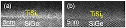
Although traditional Ni silicides provide low contact resistivities, fast diffusion of Ni in Si(Ge) limits its application in advanced nanoscale transistors (Fig. 1).
Yu: “Therefore, the semiconductor industry encouraged imec to start looking for new contact schemes and new silicide materials, exhibiting ultralow contact resistivity and compatibility with CMOS processing.”
The need for an adequate test vehicle
What was missing in the industry was a test vehicle that could accurately measure and evaluate structures with contact resistivities as low as 10-9 Ω cm2.
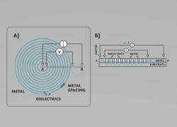
Yu: “In the frame of my Ph.D. study and with the help of the imec contact module team, I designed a unique planar test structure, based on a multiring circular transmission line model (MR-CTLM). The new test vehicle has a simple structure (with minimal process induced dimension errors), a large sampling capacity, and a high reproducibility—allowing accurate characterization of ultralow contact resistivities.” (Fig. 2).
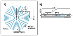
Several major foundries have meanwhile accepted and implemented this MR-CTLM test structure. The structure was also reproduced by a number of universities. The MR-CTLM has enabled accurate investigations of ultralow contact resistivities that are close to the industry target. The simple fabrication of the MR-CTLM structure has also greatly facilitated and accelerated evaluation of various industry-relevant source/drain contact schemes.
Can metal-insulator-semiconductor contacts lead to low contact resistivities?
Several years ago, metal-insulator-semiconductor (MIS) source/drain contacts started to receive much attention.
Yu: “It was shown that inserting an ultrathin insulator between the metal and the semiconductor could help achieve a very low Schottky barrier height, and this should lead to low contact resistivities. As a first part of my Ph.D. work, I evaluated this promising contact scheme in terms of contact resistivity and CMOS compatibility—for 7nm and beyond CMOS. I screened several insulator materials, including titanium (Ti)-dioxide. I found, however, two main drawbacks of the MIS source/drain contact approach, which prevented the application of MIS contacts into advanced CMOS technologies. The problems are independent of the insulator candidate.”
One of the issues relates to the thermal stability of the MIS contacts, especially on n-type semiconductors. As a second issue, on the highly doped semiconductors that are relevant to the source/drain of the CMOS transistors, the Schottky barrier lowering benefit of the MIS contacts cannot compensate the insulator tunneling barrier induced blockage of carriers.
Novel titanium silicidation techniques
As a second part of his Ph.D. work, Hao Yu switched to metal-semiconductor source/drain contacts, with Ti silicides on the metal side, and highly doped Si (n+) and SiGe (p+) on the semiconductor side. After internal discussions and in close consultation with imec’s CMOS program partners, they developed three new techniques for titanium silicidation, with improved metal-semiconductor interfaces. With all three techniques, ultralow contact resistivities in the order of 10-9Ωcm2 could be achieved – as revealed by the proprietary MR-CTLM test vehicle.
The main difference between the techniques is the compatibility with state-of-the-art CMOS manufacturability.
Yu: “The conclusions we draw from the first technique allowed me to work out a second technique—which was better in terms of CMOS compatibility. The third came from the conclusions of the second one, and is most compatible with CMOS manufacturing. All three techniques were also evaluated by our partners.”
In a first technique, called pre-contact amorphization implantation, a Ge ion implantation step precedes the Ti deposition and contact formation. This step is known to improve the Ti-silicide nucleation and crystallinity. The lowest contact resistivity values were however achieved with silicides that were not fully crystalline, but in an amorphous state with embedded small Ti-silicide crystallites.
Yu: “The particular phase of low-ρc Ti silicides inspired me to develop a second technique, based on a TiSi co-deposition to form Ti silicides. With this technique, Ti-silicide crystallite formation can be enhanced. This technique also allowed us to improve the quality, reliability and reproducibility of the source/drain contacts.”
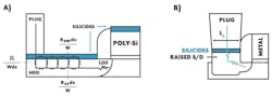
Finally, a third technique was developed to answer the limitations of the TiSix deposition technique for compatibility with CMOS processing (Fig. 3).
“Conformal chemical vapor deposition (CVD)/atomic layer deposition (ALD) TiSix would be an optimal contact solution to the industry, but the technology is still under development. As a pioneering step, together with the industrial vendors, we explored the use of conformal deposition techniques such as ALD for depositing Ti”, adds Yu. “This technique allowed us to create ALD Ti-based source/drain contacts, with ultralow ρc of 2x10⁻⁹ Ω cm2.”
In the near future, Yu will use the knowledge obtained in this Ph.D. work for developing contact schemes for III/V-based devices, such as InGaAs or GaN—in the framework of imec’s high-speed analog/RF program for 5G mobile handsets.
About the Author
Hao Yu
Hao Yu received his B.S. and M.S. degrees in Microelectronics and Solid-State Electronics from Fudan University in 2010 and 2013, respectively. He received the China national graduate student scholarship award and Shanghai excellent graduate student award in 2013. Hao Yu is now a Ph.D. candidate affiliated to imec and Katholieke Universiteit Leuven under supervision of Dr. Marc Schaekers, Dr. Nadine Collaert and Prof. Kristin De Meyer. He has been working on metal-semiconductor contact resistances and semiconductor junction characterizations. As high contact resistances become major obstacles that compromise performance of modern CMOS devices, Hao Yu has developed high-accuracy test vehicles and reported multiple contact schemes meeting the 10–9Ωcm2-contact-resistivity industrial target. He has authored and co-authored 17 articles to peer-reviewed journals and 16 to international conferences. He received the IEEE electron device society Ph.D. student fellowship award in 2017, the imec PhD student excellence award in 2018, and the China scholarship council award for outstanding self-financed students abroad in 2018. Since September 2018, Hao Yu has joined Dr. Niamh Waldron’s team at imec as a researcher working on IIIV-on-Si RF technologies.
Comment About the Article
To join the conversation, and become an exclusive member of Electronic Design, create an account today!

Leaders relevant to this article: