MEMS technology is transforming high-density switch matrices
Download this article in .PDF format.
Electromechanical relays (EMR) and reed relays have served automated test equipment (ATE) applications well, but they’re not likely to satisfy their needs in the future, as ATE manufacturers strive to increase channel densities in a smaller system footprint and as more tests need to be performed, faster, on devices under test. The answer lies in MEMS switch technology that, after years of development, has transitioned to commercialization thanks to advances in materials, fabrication, and packaging.
What took so long?
So, why is it that MEMS switches are just now appearing? It’s not for lack of trying, as many companies worked feverishly to develop MEMS switches for decades. Most fell by the wayside for lack of funding, acceptable fabrication processes, access to advanced materials, and the inability to solve crucial problems such as contact reliability, actuator deformation, and effective hermetic packaging.
The solution to these and other obstacles came from General Electric, which—beginning in 2004—took on the challenge of finding an alternative to the mechanical relays it relied on for use as high-power circuit breakers. Of the two basic types of MEMS switch technology, capacitive and ohmic, GE focused on ohmic. Other companies, principally Analog Devices, also use ohmic technology, while companies like Cavendish Kinetics and Wispry use the capacitive approach.
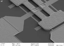
The primary failure mechanisms in ohmic MEMS switches are metal fatigue of the MEMS actuator (cantilever) and contact wear. Even though metals are excellent conductors, when used as cantilevers they deform over time and exhibit variations in temperature. After researching many materials combinations, GE realized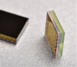
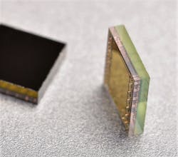
By eliminating wire bonds and replacing them with short metallized vias, TGV reduced package parasitics by more than 75%, allowing the switches to be housed in wafer-scale packages 60% smaller than wire bond packages. In addition to increasing channel density and reducing cost, TGV also dramatically decreased electrical losses while increasing linearity—key metrics for ATE applications from low-power signal switching to RF and microwave testing.
The advances proved successful in its first applications: GE’s MRI and FRMI medical imaging systems and hundreds of thousands of these switches have been delivered into those systems as of today. In 2016, GE spun off its MEMS capabilities, creating Menlo Microsystems, Inc. (Menlo Micro), which has continued to advance this work. The result today is what the company calls Ideal Switch technology, and its first new products targeted for test and measurement applications became available in 2018.
Time for a switch
EMRs and other mechanical switches are large, have limited channel density, suffer from relatively rapid contact wear, and are susceptible to environmental stresses like shock and vibration. As the size of the cantilever in an EMR is large and heavy (in relay terms), the time required for it to reach the contact to make or break the circuit is long, limiting its potential switching speed. While a MEMS switch also uses a mechanical approach, it is a microelectromechanical device fabricated in a wafer-level manufacturing process in a semiconductor fab. Its cantilever weighs almost nothing, and can switch in 10 µs rather than the 10 ms or so required by EMRs. This 1000-times reduction in switching time has major positive benefits for switch matrices, such as reducing the cost-of-test, which is primarily limited by test time.
One of the more remarkable characteristics of MEMS switch technology is that even though the components within the devices are incredibly small and light, they can nevertheless be arranged to handle hundreds of volts and tens of amperes, while requiring just a few picoamps for actuation.
With advances in electrodeposited alloys and other material innovations, the reliability and longevity issues that have plagued MEMS switch developments in the past have been eliminated. Menlo Micro’s current devices, for example, can operate for a minimum lifetime of 3 billion operations and typically greater than 10 billion. With future advances in materials and processing, this metric will be increased to greater than 25 billion operations in the next few years. In contrast, EMRs have operating lifetimes typically less than a few million operations while reed relays can last for a few hundred million operations. While a few hundred million switching cycles might seem enormous, switch matrices in many ATE applications operate at hundreds of cycles per second, so the ability of MEMS switches to operate far longer means they will likely long outlive the system itself.
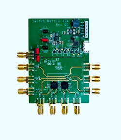
The board uses two of the MEMS switches in series as a 3x4 switch matrix with 12 cross-points (six per device). Every switch in the matrix is individually controllable, so the matrix can be configured as one to many, many to one, or can loop a signal back for testing. The evaluation board includes a microcontroller for the interface and control circuit, as well as a 75 VDC generator for actuating the switches.
The switch matrix can accommodate positive or negative AC and DC voltages alone or in combination, and is accompanied by Windows software that lets designers connect various points in the matrix and shows switching configurations. To create a larger switching environment, several boards can be connected to form 3 x 8 or 3 x 12 matrices.
Summary
The signal and power switching systems, which are often required for high-volume automated testing, are sometimes overlooked—but they are critical ingredients that play an outsized role in determining overall measurement system performance and cost. Like all electronic devices, EMRs and reed relays, the mainstay of current ATE switching systems, have limitations that directly impact the overall cost-of-ownership and cost-of-test.
That said, MEMS switch technology has been problematic for decades and has only recently surmounted its most vexing challenges, allowing them to replace EMRs in many of their core applications. In addition to switching low power and low-frequency signals, MEMS switches can now handle kilowatts of power
Chris Giovanniello is senior vice president of worldwide marketing at Menlo Micro, overseeing all aspects of technology innovation and leading product development efforts.
