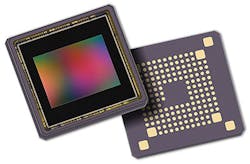
FRAMOS offers ON Semiconductor’s XGS imagers with HiSPi interface
FRAMOS has announced that ON Semiconductor has expanded its high-performance XGS family of Global Shutter CMOS image sensors with two new models: the XGS 9400 and the XGS 8000. These devices provide resolutions of 9.4 and 8.8 megapixels, respectively, in a compact package, achieving high-speed performance in a single formfactor. Both models are suited for integration into 29-mm x 29-mm-cameras for machine-vision, ITS, security, medical, and scientific applications.
Sibel Yorulmaz-Cokugur, sensor expert at FRAMOS, says, "Power consumption and heat generation are important considerations for embedding vision into industrial vision systems. Both new XGS imagers only require < 1 W at full speed and full resolution. Also, they provide stable performance over wide range of operating temperatures from -40°C to +85°C, which makes them great candidates for environments exposed to weather and sunlight."
The imager’s frame rate in high-speed mode achieves a maximum of 128 frames per second (fps) at 12 bits over 24 lanes in the 8-MP version and 90 fps in the 9.4-MP version. The frame rates of both models can be reduced to 80 fps or 56 fps in low-speed mode by companding the bandwidth and implementing only 12 lanes. The high speed, 12−bit output can maximally leverage interfaces like USB 3.2, Thunderbolt 2, and 10 GigE for industrial environments.
Image data is output through a column ADC architecture and is transferred over a HiSPi interface. The on-chip logic, which is programmable through the serial interface, generates internal timing for both integration and readout control. Up to 8 regions of interest (ROI) can be defined to reduce the data load and conserve lane capacity. Up to three register configurations can be programmed and sequentially enabled (frame-by-frame) with a single command over the control interface.
FRAMOS is available to support customers with the integration of these new sensors into their applications and projects. Evaluation kits contain the sensor, a headboard, frame buffer, and base board. In addition, FRAMOS provides services like development support, customization, and logistics. Currently, the sensor is in production mass release.
About the Author
Voice Your Opinion!
To join the conversation, and become an exclusive member of Electronic Design, create an account today!

Leaders relevant to this article:

