What’s All This Talk About Density?
Download this article in .PDF format.
In the world of test, smaller is better, provided the system can test my particular devices under test (DUTs). There are many reasons to look at smaller footprints in test—manufacturing floor space, shorter cable lengths, and portability come to mind.
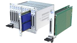
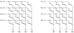
In the world of signal switching and test, the word is not necessarily smaller, but denser. Switching density is always a subject for debate as to how much switching is necessary, particularly in modular test systems because of the fixed physical size of modular devices. In this short article, we will take a brief look at some of the advantages of high-density switching and some sample applications that benefit from it. For brevity’s sake, this article will focus on crosspoint matrices. The purpose of a crosspoint matrix is to allow any number of multiple signal inputs to be connected to any number of signal outputs—basically any test resource to any test point on one or more DUTs. A 1-wire crosspoint matrix uses an array of SPST relays to close an X to Y path. In Figure 1, with path Y1 to X1 closed (green path, right image), a stub appears (red) on the line which limits the matrix bandwidth.
Advantages of density
It is important to note that higher density designs typically require that signal-carrying traces on the PCB be placed closer together; this accommodates the increase in relay count, which can increase channel-channel crosstalk.
Now let’s see a few applications that benefit from a high-density switching system.
Semiconductor test
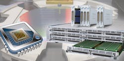
For years, IC chips have been getting more complex, and consequently, so have the test systems that verify the operation of these chips. That complexity comes at a cost—several million dollars per tester is not out of the question. As a result, chip manufacturers are always looking for ways to lower their cost of test. True,It turns out that many analog tests can be set up using a very large matrix (Figure 3), a pulse generator, and one or more SMUs (source/measure units). Now, I emphasize a large matrix because of the sheer number of test points on a wafer or pins on a device—1,000 connections at any one time is typical today.
The testing we are talking about here is aimed at characterization and validation of wafers and chips/dies in product development and NPI (new product introduction). Here are some of the tests used:
Wafer-level test can test for shorts/opens and capacitance.
IDDQ testing is a method for testing CMOS integrated circuits for the presence of manufacturing faults. It relies on measuring the supply current (IDD) in the quiescent state (when the circuit is not switching, and inputs are held at static values). The current consumed in this state is commonly called IDDQ for IDD (quiescent) and hence the name.
For chip-level as well as wafer testing, there is I-V testing for transient charge trapping. One version of this test is called SPCT (Single Charge Pulse Trapping). SPCT uses a pulse generator to do fast I-V curves to either avoid charge trapping or measure charge trapping as a function of a device’s switching frequency. With some modeling work, SPCT can distinguish the initial charge-trapping centers from those created later by voltage stresses.
One important thing to note is that in many of these tests, a large number of test points must be connected to ground to provide a stable test environment. So, it is essential that the matrix you select should be able to close a large number of the matrix’s relays simultaneously. The number of relays will depend on the product you are testing.
Board test with multi-up fixtures
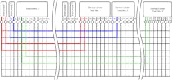
In this case, a large matrix is ideal to share resources between each DUT. In Figure 4, you see several DUTs connected to the X-axis of a crosspoint matrix. A number of instruments are also connected to the X-axis. The colored lines show a number of simultaneous instrument connections. The number of connections is limited by the number of Y-axis lines available. Once measurements are made, the matrix can reroute the instruments to other DUTs and repeat the measurement made earlier.
Board test with multiple test programs
This type of situation is where a crosspoint matrix can make your test system much more flexible as it can connect every test resource to any DUT test point, rerouting resources programmatically.
Conclusion
There are many test strategies that depend on the type of test to be performed, volume and mix of DUTs, and your budget. Clearly, no one test system can do it all, at least not economically. But if you have testing needs similar to what has been described here, a crosspoint matrix may be an important part of your test plans.
REFERENCES
“Iddq testing,” Wikipedia.
Rubin, Dave, “Short Pulse Testing Mandatory for Semiconductor Reliability,” Keithley Applications Note, 2006.
“Pickering Interfaces LXI High-density Matrix Modules Selected for Opens and Shorts Testing of Semiconductor Packages,” Pickering Interfaces Knowledge Base.
SwitchMate, 2nd edition, Pickering Interfaces, 2019.
