Special Report: Semiconductor Test
Software
Mentor, a Siemens Business, addresses silicon test and yield analysis with its Tessent product suite. “Tessent offers software products in three areas of semiconductor test,” according to Ron Press, technology enablement director, Tessent. First is DFT for logic insertion, mostly at RTL for BIST, embedded scan compression, scan, device-level DFT infrastructure, and on-chip clock controllers. The second area addresses safety, with in-system test managers and automotive-grade pattern generation. The third targets operations with tools to help with silicon bring-up and tools that apply machine learning to production test results to improve product yield.
Press elaborated on the Tessent approach to the three areas. “DFT used to be disparate tools,” he said. “Our products are designed to handle huge and complex semiconductor designs, and Tessent includes all DFT functions under one tool with one database.” There is much more intent-driven automation, since DFT products share information between them, and DFT intent is passed up the plug-and-play hierarchical DFT structure.
Press added that Tessent Safety includes BIST Observation Scan Technology, that can execute LBIST tests five times faster when in system operation. “Tessent Safety also has a partnership with ARM to provide a safety island flow. Finally, he noted that Tessent Operations embraces partnerships with ATE companies. “Tessent works closely with the majority of leading silicon providers to develop silicon-proven cell-aware diagnosis and machine-learning technologies.”
When asked about what devices the Tessent tools address, Press said, “All devices need an RTL-based hierarchical DFT flow, this is especially true for complex devices such as AI/machine-learning applications. Tessent is a true hierarchical platform that enables DFT and ATPG to be completed at the core level, and automatically retargeted through the hierarchy to the top. A top-level integrator doesn’t need to know the DFT of the core, they just need to know the intent of the test they want to apply, and the core is automatically configured for that test mode.”
ATE systems
According to Ken Lanier, principal technologist at Teradyne, the company offers several high-volume production-test products to address the complete flow for semiconductors, including the UltraFLEX and J750 families of test systems for wafer- or package-based SOC IC test, Eagle test systems for power management and discrete semiconductor test, Nextest Magnum systems for DDR and flash-memory test, LitePoint RF test systems for system-level and module test, and Titan systems for semiconductor system-level test (SLT).
“Teradyne’s solutions are optimized for high-volume production testing of complex SOCs, memory and power ICs, SIPs, and modules,” Lanier said. “Teradyne also provides hardware and software capabilities for rapid device bring-up in the case where our customers need to get billion-transistor devices from first silicon to customer samples in what could be a matter of days. Teradyne needs to blend seamlessly into existing DFT and EDA ecosystems to become an integral part of the simulation and debug process.”
Lanier commented that Teradyne’s products cover the spectrum from high-power switching components used in electric vehicles, to processors and ASICs used for server-based AI and machine-learning applications. “The two most significant challenges our customers are facing now are the faster-than-expected deployment of 5G millimeter Wave (mmWave) technology and the build-out of new server technology that makes use of specialized processors and ASICs that can draw up to 1,000 A of core power during test. This has driven the development of automatic test equipment (ATE) instrument options that enable multisite test of devices at tens of GHz or hundreds of watts.”
David Hall, director of semiconductor marketing at National Instruments, said their test solutions serve both R&D lab use and production. “In the lab, many engineering organizations utilize automated test systems that combine PXI modular instruments and NI measurement software,” he said. “In a typical test configuration for an RF semiconductor device like a front-end module, the instrumentation will include NI’s RF vector signal transceiver measurement hardware and NI’s RFmx measurement software for 5G or WLAN devices.”
For production test applications, Hall said, NI utilizes the same instrumentation and software inside of the NI semiconductor test system (STS). “STS offers a higher level of production readiness than standalone instruments—combining native calibration, load board interfaces, and other test-cell integration features for semiconductor manufacturing test,” he commented. “Many semiconductor organizations will employ STS either at wafer-level test or for packaged part testing.”
Hall said engineers can use PXI or STS products to test a range of devices, but NI is heavily targeting device types with challenging analog—and especially RF—measurement requirements. “With RF, next-generation technologies like Wi-Fi 6 and 5G require demanding measurement performance—both in the lab and in production. One of NI’s key differentiators in this space is the ability to provide lab-grade instrumentation at a production-worthy measurement speed.”
Hall continued, “Engineers in device characterization applications often see significant benefits from improvements to measurement speed—as these can often shave weeks off characterization times and significantly improve test coverage. In production-test environments, NI’s ability to deliver R&D-grade measurement accuracy enables test engineers to guarantee more stringent device performance metrics. This has become especially important in RF devices for Wi-Fi 6 and 5G, as these devices continue to introduce increasingly challenging measurement requirements.”
Semancik described the ATEasy test-development environment with the ICEasy integrated test executive and a semiconductor test tool suite as another unique aspect of the GENASYS Semi platform. “ICEasy, which is supplied with all GENASYS Semi systems, offers a comprehensive suite of software tools for semiconductor test applications including digital file translation and AC/DC test tools including shmoo plots and I-V curve plotting,” he said.
Semancik described the GENASYS Semi as a scalable PXI-based test platform that provides flexibility and functionality suitable for testing a broad range of devices. “Leveraging the open architecture of PXI and the TS-960e platform, systems can be configured for test applications including RF, digital, 5G beamforming devices, gas sensors, and SoC devices,” he said.
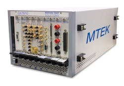
The company also offers the MTEK (Marvin Test Expansion Kit) Series. “Based on Marvin Test Solutions' portfolio of PXI chassis and instrumentation, the MTEK Series can be readily integrated with a legacy ATE platform, providing advanced digital, analog, or RF test capabilities,” Semancik said. “Based on the open architecture of PXI, the MTEK system offers a flexible and scalable solution which can be specifically configured to address a range of test needs for both packaged and wafer test applications.”
Instruments and systems
Lörner commented on several aspects. “For on-wafer characterization of RF and millimeter-wave components, Rohde & Schwarz has collaborated with MPI in Taiwan for a number of years, offering turnkey solutions for measurements on semiconductor components,” he said. “Our network analyzers support frequencies up to 110 GHz, with frequency converters extending the range up to 1,100 GHz. They work in conjunction with MPI wafer probers, in all-in-one solutions designed for precision analysis of 150- and 200-mm wafers.”
The probers include the TS150-THZ, which Lörner called the first 150-mm-wafer dedicated probe station designed explicitly for mm-wave and THz on-wafer measurements. The TS200-THZ for 200 mm wafers adds active impedance tuner integrations, providing accurate tests for the combination of requirements for mm-wave, THz, and automated impedance-tuner applications.
Rohde & Schwarz cooperates with MPI on yet another application. “For antenna on-chip measurements scanning the antenna pattern in the far field at frequencies from 50 to 500 GHz, R&S ZRX mini-receivers are designed for situations where weight and size are critical parameters,” Lörner said. “R&S offers turnkey solutions for antenna on-chip measurements, including R&S ZRX mini receivers coupled to horn antennas and mounted on a robot arm, vector network analyzers R&S ZNA or R&S ZVA for analysis, and R&S QuickStep software for antenna pattern visualization.”
Rohde & Schwarz also cooperates on load-pull measurements of power-amplifier chips running under compression, where they can exhibit nonlinear behavior due to impedance differences and reflection effects. “R&S partners Focus Microwaves and Maury Microwave provide packages featuring R&S ZNA, ZNB, and ZVA network analyzers for load-pull measurements from 10 MHz to 110 GHz,” Lörner said.
ESD is another area that Rohde & Schwarz addresses. “With the increasing miniaturization of structures in semiconductor chips, the susceptibility to damage caused by electrostatic discharge increases. Intelligent electrostatic protection for the pins of integrated circuits are an essential task for layout designers. Together with High-Power Pulse Instruments GmbH (HPPI), Rohde & Schwarz supplies a system to test electrostatic protection circuits.”
He explained that the circuit under test is subjected to high voltage pulses, with the resulting signals captured by an R&S RTP oscilloscope, which can measure pulses with rise/fall times of picoseconds up to the full bandwidth of 16 GHz, with flexible trigger functions. HPPI software tools provide analysis.
Lörner also commented on automotive radar chip testing in the 77/79-GHz bands. “The R&S ATS1500C antenna test chamber features a CATR (compact antenna test range) reflector using indirect far-field technology, to provide a high-quality 30-cm quiet zone within its1.3-m2 footprint,” he said. “The radar sensor fixer and positioner provide simultaneous movement in azimuth and elevation, to accurately simulate radar and object movement, with an angular resolution up to 0.03°.”
He continued, “The R&S AREG100A automotive radar echo generator meets all significant automotive industry requirements to generate echoes for radar sensor production test and car assembly-line calibration, including 4-GHz bandwidth, plus a simple method to include interference from an additional source. The R&S AREG100A simulates distance with an accuracy of up to 0.1 m.”
Lörner identified a trend toward mmWave and THz on-wafer testing for both power amplifier chips and antennas-on-chips for frequencies from 50 to 500 GHz. He also cited K-band devices—5G FR2 consumer and network infrastructure equipment; satellite-communication, microwave-link, and network-backhaul equipment; and traffic speed detectors. “24-GHz automotive radar is still generating test requirements,” he said.
Also generating test requirements, he said, are devices operating at 5G FR1 frequencies, both cellular and noncellular IoT, and wireless personal network technologies such as Bluetooth, LoRa, and ZigBee. So too, he said, are power-amplifier chips using technologies such as GaN, GaAs, and LDMOS.
“For investigating switching losses in MOSFETs or IGBTs, engineers use the double-pulse-test method to evaluate thoroughly dynamic behavior at power up and power down,” Lörner said. “Performing this test requires generating at least two voltage pulses with varying pulse widths and precise timing.” He said the R&S RTO oscilloscope includes both an optional pulse generator and a high waveform update rate, with up to 16-bit vertical resolution for high precision measurements.
“The R&S RT-ZHD family of high voltage probes features excellent DC accuracy (0.5%) and includes the R&S ProbeMeter built into the probe head for instantaneous DC measurements without removing the probe,” he said “The 2,000-V offset compensation is the largest available. We believe the damage-preventing over-range indicator for both input and common mode is unique on the market.”
Hauck said customers are looking for increasing bandwidth and upper frequency of operation to test advanced 5G performance parameters. “5G New Radio protocol requires bandwidth as high as 400 MHz in a single modulated channel, and AR amplifiers provide the needed broadband coverage.” He added that AR offers high reliability, with RF outputs immune to device short/open conditions, and he noted that high-power amplifiers can be split to test multiple devices at the same time to support test-time reduction.
ESD test is the focus of ESDEMC Technology. “We offer ESD test equipment from ESD simulators to fully automated TLP systems,” according to Michael Reardon, design and application engineer. “Customers use our equipment to characterize their semiconductor devices and test for ESD immunity.” Customers, he said, use the company’s equipment to test devices ranging from 2-terminal ESD protection devices to ICs having more than 100 pins.
When asked what features customers ask for, Reardon said, “Higher levels of test automation are always desired by the customer, especially for those who perform large quantities of tests. Automation is a key factor in helping to reduce testing time, effort, and cost.” He added, “ESDEMC makes an effort to customize each system such that the customer gets exactly what they need at the lowest cost possible.”
Copper Mountain Technologies offers compact USB vector network analyzers that use an external computer to deliver S-parameter measurement data, according to Brian Walker, senior RF design engineer. He added that the company’s VNAs can easily be integrated into ATE systems. “The analyzer takes up less space and is more cost-effective than comparable VNA options, with a reduction in test-time latency, while working on the same computer that is running ATE automation scripts.”
Walker added that the company’s VNAs are useful for analysis and verification of RF circuits in a variety of frequency ranges. “Our team of specialists are always available to support the integration of our equipment into the customer’s test system,” he said. “For instance, our millimeter-wave extenders may be mounted directly on probe-station arms or located in close proximity to the wafer test fixture to reduce loss and improve measurement accuracy.”
“Ophir RF makes high-power RF amplifiers for doing RF testing of semiconductors in the GSM, UMTS, TDMA, EDGE, i-DEN, PCS, ZigBee, WLAN, Wi-Fi, EV-DO, WCDMA, LTE, 802.11.b, and Bluetooth frequency bands,” Davis said, adding that the company can also serve many other semiconductor bands. As for what features customers are looking for, he said, the never-ending quest for any amplifier product is “higher frequency, higher power.”
Keithley, a Tektronix company, offers DC characterization and test equipment for R&D, production, and off-line analysis applications, as well as turn-key software for automated wafer-level production testing. According to Brad Odhner, technical marketing manager, “our solutions range from individual instruments, to multichannel benchtop systems, to full in-line automated test systems.”
Odhner said Keithley’s S500 line of parametric test systems supports large-scale production, with support for wafer mapping, SECS/GEM, parallel test execution,
Odhner said key areas include wide-and bandgap (GaN, SiC) power devices, optoelectronics, sensors (including IoT and MEMS), display technologies, materials, memory. “Many of our products have built-in test applications to enable immediate out-of-the-box results, like the Clarius software on the 4200A-SCS, which comes with hundreds of built-in tests with real example data we’ve taken ourselves.”
“Other products are reconfigurable and scalable for redeployment as needs and/or applications change, like our 2400 and 2600 family of source measure units, where their TSP functionality allows the building of mainframe-less networks and fully automated test systems,” he said.
Odhner added the most recent addition to the company’s SMU lineup is the 2601B-PULSE PulseMeter Pulser/SMU. “It grew out of many conversations with customers, and is optimized for testing on-wafer VCSELS and other optical diodes, with autotuning 10-A, 10-V, 10-ms pulses while digitizing waveforms at 1-MS/s to allow better characterization of optical devices.”
Accessories
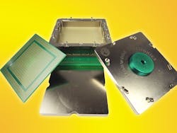
The configuration tested in the SBT-BGA-6048 can be a BGA or LGA with 70 x 70-mm body size, 1.27-mm pitch, and 54 x 54 ball array. When using the socket with a BGA, a removable ball-guide must be placed over the pin array. When testing an LGA, the ball guide is not needed. This socket can be used for hand test and quick-turn custom burn-in applications.
EE asked contributors to this report to elaborate on features, cost-of-test issues, and semiconductor test trends. Read on to see what they had to say.
What features or innovations are customers asking for in semiconductor test?
Lanier, Teradyne: “Our customers are driving innovation in two key areas: instrument technology and time to market. High-performance computing power supplies and mmWave instruments represent two of the most urgent needs in terms of test hardware. While hardware is an important enabler, most of our customers’ investment is actually in developing test programs and code libraries and integrating both of those to an EDA and DFT infrastructure that integrates the device designs directly into the silicon bring-up process. The more efficiently this integration can be done, the sooner device production can be ramped with the required quality desired by end users.”
Press, Mentor: “Many customers are asking to ease the complexity of integrating DFT for large complex designs. A major part of it is many companies requiring their IP providers to include IJTAG so the IP fits within a plug-and-play IJTAG environment as in Tessent. We also see requests to remove in-house complex scripting necessary to maintain current flows that are special to that particular company. Many of these flows are migrating to Tessent, since DFT knowledge of the tool is available to the user through introspection, for powerful scripting and the ability to register companywide DFT DRCs and commands.”
Hall, NI: “Many of the features and innovations NI’s customers are requesting relate to test requirements from next-generation wireless devices. For example, the evolution of the Wi-Fi technologies beyond 6 GHz is pushing the need for high-dynamic-range measurement requirements. With 5G, one of the most challenging requirements for test engineers is the need to test devices in an over-the-air (OTA) configuration. For 5G devices operating in the mmWave bands at 28 and 39 GHz, the physical dimensions of the antenna often make it advantageous to package the antenna and beamformer in the same physical package.”
“Testing antenna-in-package (AIP) devices is especially difficult—as the devices typically do not have a physical port where one can access the RF signal. Although NI has worked closely with many engineering labs to introduce OTA measurements in an R&D environment, many semiconductor companies are looking employ OTA measurement techniques in a production test environment. NI is continuing to partner with leading chipmakers to develop low-cost OTA solutions for production test.”
Semancik, Marvin Test Solutions: “The move to 5G devices is driving the need for higher frequency RF test capabilities; demands for parallel, multisite 40-GHz to 80-GHz test are becoming more commonplace—coupled with the demand for cost-effective production-test solutions.”
Lörner, Rohde & Schwarz: “A key feature is the integration into the complete test setup, including into fixtures in general and on-wafer test in particular, for both manual and automated test. Needless to say, test speed and ease-of-use are also key requirements.”
Walker, Copper Mountain Technologies: “Copper Mountain Technologies has found that customers require fast measurement speed while still needing accurate test results. To address this need, we offer VNAs with measurement speed as fast as 10 ms per point while still offering up to 152-dB dynamic range for our Cobalt 9-GHz VNAs and 16 ms per point with 140-dB dynamic range for our SC5090 9-GHz Compact VNA.”
Odhner, Keithley: “In general, many of today’s customers do not have time to create and maintain their own custom-built test systems and therefore are increasingly looking for complete solutions (hardware and software) at each phase of the workflow. From a measurement perspective, we are seeing needs for faster, higher-power pulsing in optoelectronic applications (hence our new 2601B-PULSE) and better performance in noisy environments, which are addressed by our latest 4200A-SCS SMUs, the 4201 and 4211, which offer enhanced performance in high-capacitance test setups.”
How do you help your customers lower the cost of test?
Press, Mentor: “Tessent provides embedded compression and special test points to reduce the test time. However, many companies struggle with knowing what the best pattern targets or mix of tests should be. Tessent recently released the ability to sort the various pattern types based on total critical area. This way the tool can choose the best patterns to detect physical defects in any part of the design. This is a dramatic step in the ability for users to optimize their test patterns.”
“Additionally, our analog fault grading helps identify unnecessary analog tests, which can greatly reduce test time. The tight integration of Tessent ATPG and Operations products allows us to increase the value of test while reducing the cost. We are working with customers to understand how to optimize their DFT designs pre-silicon, to maximize the benefits from diagnosis and yield improvement post-silicon during yield ramp and manufacturing.”
Semancik, Marvin Test Solutions: “Vendors face pressures to control costs and improve time to market, which have sparked a move to retrofit existing production test systems with expanded test capabilities—RF, digital, etc.—allowing test departments to extend the life cycle of existing test systems and leverage current test assets. Designed to support both engineering and high-volume production installations, the MTEK Series can be the ideal low-cost solution for extending the life cycle of legacy semiconductor ATE systems.”
Hall, NI: “Especially in semiconductor production-test applications, NI is increasingly helping chipmakers lower their cost of test by increasing tester site count and throughput. In fact, we often put an extreme focus on squeezing out every millisecond of test time possible through a broad range of techniques. For example, in RFIC production test applications, we employ high-end multicore processors to parallelize heavily processor-intensive modulation quality measurements. In some instances, we’ll even deploy measurement IP into FPGAs to further accelerate test time. In a typical production test application, we are able to increase test throughput by 20% to 40% versus the competition.”
Lanier, Teradyne: “Device quality and production costs go hand-in-hand. These two requirements drive us to offer instrument hardware performance that reduces the measurement error contributed by the test equipment to extremely low levels. This unprecedented level of accuracy lets our customers guarantee the performance of their devices while, at the same time, reducing the amount of ‘overkill’ that is scrapping devices that fail marginally, but in fact were good enough to ship.”
“For any devices built on 7-nm, 5-nm, or 3-nm technology, the largest driver of overall manufacturing cost is the silicon itself. This means that the most expensive thing you can do is to scrap what were actually good devices. In many cases, increasing the yield of these devices by as little as one percent can actually pay for the entire cost of testing every device. Pretty quickly, this means that test is no longer a cost, but rather a profit generator.”
“The other primary way we help control costs is to simply make test cells more productive with higher units per hour (UPH) per tester. For complex devices, ATE only constitutes about 35% of the cost of operating a test cell. The math here is pretty simple. You can pay less for the tester and save a little, or buy a faster tester and save a lot because the faster tester eliminates the other 65% of the cost of unneeded test cells.”
Lörner, Rohde & Schwarz: “We lower test costs through parallel testing, plus increasing use of non-embedded data processing and analysis on computers of the customer’s choice, whether this is a PC dedicated to the test setup, a client-server setup, or even processing in the cloud. Wherever practical, implementing functions in software rather than hardware increases the flexibility and update possibilities for equipment, which reduces costs long term.”
Walker, Copper Mountain Technologies: “In general, VNAs from Copper Mountain Technologies are very affordable. In addition, most important analysis features such as time-domain gating are available without charge.”
Odhner, Keithley: “Lowering costs requires addressing both the initial capital expense (CAPEX) and ongoing operating expenses (OPEX). In general, Keithley is known for products with high MTBF, low MTTR, and very competitive pricing. In addition, many of our products have our unique Test Script Processor (TSP) technology, which enables ultrahigh throughput to reduce test times by moving processing power from a central, bottlenecked computer into the test instruments themselves. The combination of all this results in a low overall COO (cost of ownership), which is the key metric for lowering the cost of test.”
What trends are you seeing in semiconductor test?
Hall, NI: “Although it’s difficult to call this a ‘new’ trend, we continue to see chipmakers driving an intense focus to increase the level of integration and reduce the footprint of ICs. These trends are combining to drive the prevalence of system-in-package (SIP) device integration. In addition, we’re continuing to see dramatic increases in the port counts of RFIC devices. Although many RFICs were historically more discrete, many RF devices include significant DC and digital ports as chipmakers attempt to integrate converters, power management, and other functionality into RF chips.”
Lörner, Rohde & Schwarz: “[We see] increasing integration—chips that feature a complete RF frontend from digital input on the one side to the antenna on the other; increasing frequencies, led by the K and E bands; increasing power density; [and] Increasing voltages made possible by wide-bandgap semiconductors.”
Walker, Copper Mountain Technologies: We see the need for higher frequency measurement at faster speeds and the need for more measurement ports.”
Odhner, Keithley: “The biggest trend we see is power semiconductor manufacturers continuing to push for better operating efficiency of their devices. This means lower leakage currents, lower on-resistances, and higher breakdown voltages are required. Products like our recent 2470 SourceMeter with a minimum 10 fA current resolution facilitate development in these areas by providing engineers the measurement accuracy they need to characterize these advancements.”
Press, Mentor: “Industry-wide trends of RTL-based hierarchical DFT and plug-and-play infrastructure with IJTAG are becoming even more critical in newer more complex designs, sometimes with hundreds or thousands of cores. Having a capability to connect all the DFT pieces together with automation is vital to get products to market. In addition, the GPIOs are not growing at the same rate as transistor counts. Semiconductor companies want to take the level of DFT integration and automation to the next level [and] focus on optimizing the core level DFT with the DFT infrastructure able to manage and optimize it at the design level automatically.”
Semancik, Marvin Test Solutions: “There has been an increase in customer development of application-specific test solutions with a focus on the cost of the tester and reducing the overall cost of test. This is especially true in the emerging areas, such as RF test requirements for 5G and automotive radar, where off-the shelf production test capabilities are limited or unavailable. As a result, test engineers are developing internal test solutions using open-architecture hardware and software platforms as building blocks.”
Lanier, Teradyne: “The most interesting trends are driven by new silicon processes and packaging technologies. More complex, multibillion-transistor silicon designs drive a massive amount of data volume in and out of the tester. This takes the form of hundreds of millions of test vectors that must be sourced to devices under test or used to compare device outputs. There are also hundreds, sometime thousands, of voltage and frequency trimming steps that must be performed on multiple devices in parallel. Lastly, customers want to store terabytes of test data daily to use inline or offline to optimize device fabrication and test processes. Accommodating these needs makes data throughput one of the most critical characteristics of an ATE system.
“New packaging trends can radically alter device manufacturing and test flows. The most obvious impact is an increased reliance on known good die (KGD). As devices get more complex, the fault coverage from scan testing quickly becomes inadequate. This is driving a return to more functional test on ATE to complement structural test. In many cases, dedicated system-level test (SLT) insertions can quickly become necessary. For new ‘chiplet’ designs, there is also a new challenge of testing die with extremely low-power outputs, which are normally designed to only drive signals a few millimeters, instead of driving an ATE signal path that can be the better part of a meter long. Addressing this challenge will require the complete rethinking of the electrical interface between the silicon and the ATE.”
Companies mentioned
About the Author

Rick Nelson
Contributing Editor
Rick is currently Contributing Technical Editor. He was Executive Editor for EE in 2011-2018. Previously he served on several publications, including EDN and Vision Systems Design, and has received awards for signed editorials from the American Society of Business Publication Editors. He began as a design engineer at General Electric and Litton Industries and earned a BSEE degree from Penn State.
Comment About the Article
To join the conversation, and become an exclusive member of Electronic Design, create an account today!

Leaders relevant to this article: