An 8 GHz PXI Dual SP8T Multiplexer Based on MEMS Switches
Download this article in .PDF format
Modern communication systems ranging from 5G cellular to military radios are increasingly required to support a growing number of channels and frequency bands, and it is often essential to be able to accurately and efficiently test multi-band and multi-port RF components that comprise these systems. Routing of the necessary signals will present a challenge as the number of ports needed to support these multiport components are increasing, while maintaining critically important low RF losses, fast switching speeds, and test throughput.
RF switch matrices provide automatic signal routing and conditioning between test and measurement equipment and devices under test in RF ATE systems and test benches. They can be used to efficiently connect multiple inputs to multiple outputs for test systems and route and multiplex signals between the Devices Under Test (DUTs) and test equipment and systems.
Switch matrix architecture with a twist
It is important to note that this article will focus on a variation of the traditional switch matrix architecture. In this example the design is built around eleven Menlo Micro MM5130 SP4T devices configured as a dual SP8T switch multiplexer. An important definition between a switch matrix and multiplexer is that the multiplexer can connect one input to multiple outputs, or multiple outputs to one input.
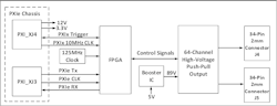
The design is configured as a single PXI card and operates up to 8 GHz and is targeting the 5G Sub-6 GHz bands, as well as general-purpose commercial RF applications. The multiplexer is integrated with an Intel (Altera)-driver controller board and all necessary biasing and high-voltage driver circuitry for the switches. The design uses 18 Mini-SMP RF connectors, and the multiplexer card is operated with a Windows software GUI to control full switch operation with Windows DLL drivers with APIs for operating the switch multiplexer with an ATE system.
The functional block diagram of the PXI Carrier Board is shown in Figure 1 below. The PXI carrier board is based on the Intel (Altera) Cyclone IV FPGA, the Altera device can support PXI Gen 1 X1, X2, and X4 (2.5Gbps) speeds. The board includes 89V power supply circuits and a 64-channel high voltage push-pull driver device which can provide DC bias to control the MEMS switches.
The MEMS switches are activated via electrostatic force, and thus require a high voltage source for switching operation. The gate of the switch is set for a bias of 0 VDC, which places the metal cantilever beam in a non-deflected (off) state. Thus, the path between RF input and output is isolated with an air gap, like a traditional mechanical relay.
When the gate is set to its required actuation voltage of +89V, the electrostatic force that exists between the gate and cantilever beam is strong enough to cause it to deflect downward, forming a connection with the contact and closing the switch (on state). Given the low supply current necessary for the electrostatic operation, a single charge pump circuit is used to generate the +89V required by the MEMS switches. The card provides two 2X17 (34-pin) connectors to allow flat cable connection to the SP8T RF boards.
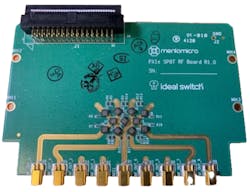
The RF board shown in Figure 2 uses eleven RF MEMS SP4T switches to realize a SP8T switch configuration. All the unused ports are terminated with a 50-ohm RF resistor. User connections are made via nine mini SMP connectors per board to accommodate two banks of nine RF connectors on a small PXI bracket space.
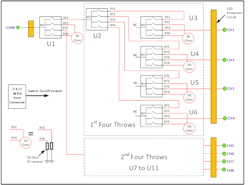
Figure 3 shows a photograph of the SP8T RF board. Six-layer PCB stack up used with Roger 4003C as dielectric layer to get optimum RF performance. The RF traces are routed on both top and bottom layers and a Grounded CPW (CPWG) transmission line is used for the design.
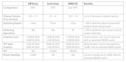
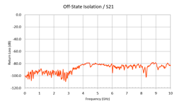
The ultra-low Coff directly contributes to this design’s target off-state isolation of 80 dB. Switching on-off operation is less than 20us and this is typically a 750 times improvement over competing relay-based switches. One strong point of traditional EM solutions is that they often have total lower insertion losses through the switches and matrix, but the tradeoff is that they have much shorter operating lifetimes. This is also apparent when operating an EM-based system at higher power levels, often referred to as “hot switching” and EM relays exhibit even shorter operating lifetimes under higher RF power levels.
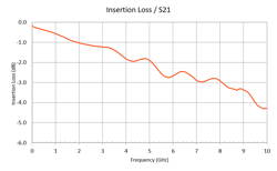
The other comparison is to solid-state switch-based multiplexers or matrices. While switching lifetimes are usually much longer than EM or MEMS-based switches, their insertion losses are usually noticeably higher and limited in RF input power levels due to device compression curves and lower linearity. Table 1 shows the specification of the MEMS-based PXI Dual SP8T multiplexer module compared with typical EM or solid-state designs. Key performance benefits are in the areas of insertion loss, size, weight and power consumption, as shown in Figures 4 and 5.
Looking forward
In summary, this novel design example for a PXI Dual SP8T Multiplexer demonstrates how the use of MEMS switches can eliminate many of the compromises that are necessary when working with either EMR or solid-state switching technologies. Given the small size, there are many improvements that will be possible in the near future.
Current research and development is focused on (1) delivering considerably lower loss with optimized designs, such as “switch-matrix-in-a-package”, (2) the ability to provide both reflective and terminated versions, and (3) extensions to mmWave frequencies, up to 50 GHz. In addition, while the channel count is currently limited by the connector interface on the PXIe platform, the miniature size of the MEMS switch allows for the creation of much higher density switch matrices, to hundreds of channels, in custom assemblies.
With the seemingly endless proliferation of new frequency bands, for both commercial 5G and military systems, the complexity of the test systems will continue to increase. The ability to have an RF switch multiplexer that not only meets the RF performance requirements, but also saves crucial space in the PXI chassis, will provide a big efficiency savings for test engineers. In addition, the MEMS-based approach provides significant cost of ownership reductions over EM solutions given the significantly higher reliability and switching speed.
