Conformance test failed. What now?

Conformance tests are performed on serial data interfaces such as USB, HDMI and PCI Express to ensure interoperability between electronic devices and accessories. In cases where signal integrity problems are encountered, modern oscilloscopes support root cause analysis by providing powerful tools such as eye diagrams, jitter and noise separation as well as time domain reflectometry.
Automatic conformance tests for high speed data interfaces
Conformance tests represent an important milestone during product development. The relevant standardization committees have published detailed test specifications for many interfaces such as USB and Ethernet. Specialized test labs offer complete testing services for such interfaces, including documentation and certification. For users who need to perform these tests on their own, modern high-performance oscilloscopes provide automated test solutions for all common interface standards. These solutions are equipped with graphical measurement configuration tools and off-shelf test sequences. No matter how the testing is performed: If results do not comply with the standard, time-consuming debugging is required.
During root cause analysis, the oscilloscope provides support with analysis tools such as eye diagrams with mask tests or separation of jitter and noise components. Time domain reflectometry is also available for verifying the transmission characteristics of passive signal path components such as connectors, cables and signal lines on the printed board.
Conformance testing for USB 3.2 transmitters
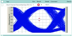
USB 3.2 transmitter conformance testing focuses on the eye diagram (transmitted eye) for verifying the eye opening, signal levels and jitter components. This test is performed directly on the device output (short channel) as well as with a simulated signal path (long channel). For long channel tests, the USB Implementers Forum (USB-IF) has published files with S-parameters for various cable and signal trace lengths. During the tests, the oscilloscope acquires clock and data signal sequences with a length of 200 µs. These sequences are then checked for compliance with the standard using the SigTest USB-IF analysis software. Depending on the test mode, each USB device must generate the compliance patterns on its own: For USB 3.2 Gen 1, this means patterns CP0 (data) and CP1 (clock) and for USB 3.2 Gen 2, patterns CP9 (data) and CP10 (clock). Switching to the next CP pattern involves sending short LFPS sequences to the receiver in the USB device.
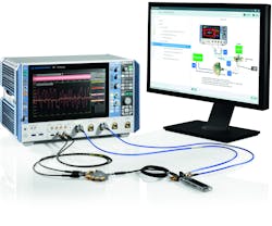

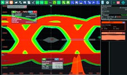
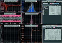
Fig. 3 shows an example of errors that occurred during the transmitted eye test for a USB 3.2 Gen 1 device. The random jitter (RJ) determined with the clock pattern (CP1) is especially noticeable. The corresponding eye diagram for the data pattern (CP0) also exhibits high jitter and noise. The analysis tools provided with the R&S RTP make it possible to investigate the root causes of these problems.
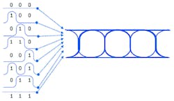
Eye pattern analysis is one of the best-known techniques for performing fast signal integrity tests. It involves superimposing the individual data bits of a signal sequence (Fig. 4). Selection of the appropriate timebase for bit analysis is critical here. For all USB standard generations, 2nd order clock data recovery (CDR) is defined with different transfer functions.

Resolving error sources due to jitter and noise components
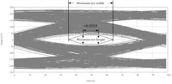
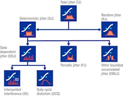
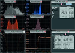
A histogram in the eye diagram can provide initial insights into the jitter and noise contained in the test signal. However, in order to gain more detailed information about the interference sources, it is very helpful to break down the total jitter and total noise into the individual components (Fig. 7).
In addition to analyzing the active signals, it is also important to check the signal paths in case of signal integrity problems. Here, the focus is on the transmission losses as well as the impedance response and stability along the signal path. Depending on the signal, the bandwidth of the signal paths on the printed board, the connectors, the cables, etc. requires appropriate design and selection. Impedance steps should also be avoided due to the reflections they can cause.
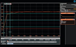
The relevant measurements are usually performed using network analyzers. The R&S RTP with integrated time domain reflectometry (TDR) provides a useful alternative. The differential 16 GHz pulse source is used as a stimulus; its reference outputs allow measurement of the reflected signals with the oscilloscope channels.
The application software provides support during setup calibration as well as during the measurement. TDR can be used to measure the impedance and reflection coefficient along the signal path.

Summary
Conformance tests on serial bus interfaces include important measurements when it comes to ensuring interoperability between electronic devices and their accessories. When errors are encountered, appropriate T&M equipment is the key to rapidly determining the root causes. Along with software options for performing automated conformance tests, modern high-performance oscilloscopes like the R&S RTP provide a number of very useful tools for debugging signal integrity problems.
Guido Schulze, product manager oscilloscopes at Rohde & Schwarz, Munich
About the Author
Guido Schulze
product manager oscilloscopes at Rohde & Schwarz, Munich
Comment About the Article
To join the conversation, and become an exclusive member of Electronic Design, create an account today!

Leaders relevant to this article: