Color and Ultrasound Reveal Feature Depth in IGBTs and Other Components
What you’ll learn:
- What is acoustic micro imaging?
- How the Nordson Sonoscan AMI tool images IGBTs, stacked wafers, and flat-surface items.
Acoustic micro imaging (AMI) is used to screen or analyze insulated-gate bipolar transistors (IGBTs), flip chips, power devices, ball-grid arrays (BGAs), ceramic chip capacitors, and numerous other component types. The purpose of scanning is to create an acoustic map, in color, of internal features to identify structural defects without physically opening the component. Defects are often air-filled cracks or voids. The color will reveal the depth of a defect.
The transducer of an AMI tool scans horizontally just above the surface of a multilayer electronic component. It fires a very brief pulse of ultrasound downward through the 3-mm layer of water that enables the pulse (which doesn’t travel through air) to reach a single tiny x-y location on the top surface of the component. The pulse travels through the 3 mm of water at about 1498 meters per second, so this step takes about 2 µs.
When the pulse strikes the water-to-solid interface, a portion of its energy is reflected back toward the transducer. There, its arrival time is noted and the distance from the transducer to the water/solid interface is calculated and saved as a reference for subsurface inspection.
At every x-y position, the portion of the pulse that’s not reflected travels deeper into the component, where it may be reflected by additional material interfaces. The moving transducer performs the whole operation—launching pulses and receiving echoes—tens of thousands of times per second. Each pulse/echo will provide one colored pixel for the acoustic image.
Ultrasound
Ultrasound isn’t reflected from the bulk of homogeneous materials, but rather from the interface between two different materials. A pulse striking an interface sends back an echo whose amplitude is determined by the relative acoustic properties of those two materials. If the two materials are both solids, the percent of the pulse’s energy reflected may be from a few percent up to about 60%.
The non-reflected part of the pulses’ energy crosses the interface and travels deeper into the component, where it may be reflected from interfaces between deeper materials. But if the second material is air, the pulse is virtually 100% reflected back toward the transducer. None crosses the solid-to-air interface.
IGBT Imaging
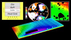
Figure 1 shows how the Nordson C-SAM Acoustic Micro Imaging tool can image an IGBT to find voids and other defects that may cause electrical failures during use. Sonoscan technicians point out that users will avoid scanning the top surface of the IGBT because even very slight residue left by the water coupling could cause damage during operation.

However, an inverted version of C-SAM pulses ultrasound into the heatsink on the bottom surface of the IGBT to generate echoes from various internal interfaces. The red lines in Figure 1 mark the top and bottom of the gate from which echoes are accepted for imaging. Echoes reflected from higher and lower depths are ignored.
Note that the gate in Figure 1 begins just above the heatsink-to-solder interface, because echoes from this interface would have no useful information. But it ends just above the solder-to-raft interface to pick up all of the raft’s contours.
Within the solder layer, a single void is shown above an arrow representing an echo reflected from the solder-to-air interface. The pulse striking the void is reflected as an echo whose arrival time at the transducer reveals the depth of the void.
The IGBT shown in Figure 2 was imaged in this way using the 30-MHz transducer of a C-SAM tool from Nordson Test & Inspection. Two frequent defects are voids (along with similar air-filled defects) in the solder and tilting or warping of the ceramic raft.
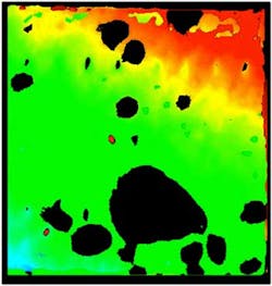
The IGBT shown in Figure 2 was imaged in this way using the 30 MHz transducer of a C-SAM® tool from Nordson Test & Inspection. When looking for defects and anomalies in IGBTs, the depth of interest often involves the solder layer between the heat sink and the ceramic raft on which the die are mounted. Two frequent defects are voids (along with similar air-filled defects) in the solder, and tilting or warping of the ceramic raft.
The diagram in Figure 1 shows the details. The color map used in this acoustic image indicates the depth of an interface. The background of this image is the interface between the solder and the bottom surface of the ceramic raft.
The deepest areas of this interface are pale blue, faintly visible in a small area at the lower left corner. The highest regions - those closest to the heat sink - are bright red, at upper right. As the interface moves upward from the pale blue region., it becomes green, pale green, yellow, orange, and then red. The boundaries between these colors suggest some irregularity in the raft’s contours.
Ultrasound is pulsed into each of the thousands of x-y locations within the area of the IGBT. Echoes are reflected by all internal interfaces within this area, but only those that come from depths that will yield useful information are collected. The first internal interface encountered by a pulse is the interface between the heat sink and the solder. All echoes from this interface are ignored, but any material interface even a fraction of a micron deeper is collected.
All of the solid black features in Figure 2 are air-filled voids just below, and likely in contact with, the heat sink. In the color map used here, black means “no echo from this x-y location.” The gate—the depth from within which echoes will be accepted for imaging—begins just below the heat sink. It does not include the heat sink to solder interface, because this interface would be the same color everywhere. The large and small voids near the top of the solder are black because their top surfaces lie just above the top of the gate. They reflected the incoming pulses before the depth at which echoes collecting began, so the echoes were ignored. Their black color means “no echo received.”
Stacked Wafer Imaging
Figure 3 is the 180-MHz image of an experimental stack of five direct-bonded silicon wafers, imaged with the color map at left. White features are the deepest; black, though lower on the map, simply means “no signal received.” The five wafers have four internal interfaces, but Figure 3 was gated to include only the first two interfaces below the surface being scanned.
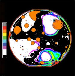
Figure 4 shows the structure of the stack in a side view. The orange rectangles represent circular holes that were drilled in one of the wafers before stacking.

In Figure 3, which images he first imaged interface between wafers 1 and 2, orange displays the tops of these features. The solid-to-air interface at the top of these features reflects essentially 100% of a pulse, even if the air in the void is only a tiny fraction of a micron thick. The non-rectangular orange features in Figure 4 are voids at the same interface between wafers 1 and 2; like the drilled holes, they’re filled with air.
Looking back at Figure 3, the numerous white features are voids between wafers 2 and 3. The additional colors seen around two of the large voids don’t represent extensions of a void into higher depths. Rather, they’re caused by local variations in the bond quality of this material.
No part of the pulse crosses the solid-to-air interface at the top of a void. If there’s another void, or part of a void, directly below this void, it will not be imaged at this x-y position.
Surface Profiling of Flat Items
In addition to measuring the depth of internal features very precisely, the AMI tool can image the surface profile of items that are flat or supposed to be flat. The basic technique is the same: A pulse is launched toward the target at each x-y location, but only the reflection from the water-to-component surface interface is collected and used for imaging. The travel time of the received echo is measured at each of thousands of x-y locations.
A color is assigned to each depth range; the resulting acoustic image is essentially a topographic map of the sample’s surface. The technique itself is known as acoustic surface flatness (ASF). If the surface is flat, all pixels will have the same color.
Figure 5 is the ASF image of a small unpopulated printed circuit board, The purpose of imaging was to determine whether differences in altitude might put dangerous stresses on components that will be mounted on the board. The color map is essentially the same as the map used in Figure 2. The lowest points are red, at the far left corner, and the highest are pink, near the middle of the front edge. The full on-board color range extends approximately from 0.120 to 0.920 mm.
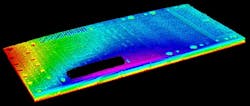
ASF is often used on bare boards to prevent stress-induced electrical defects that will sever connections. It’s also frequently utilized on large-area components such as BGAs, where surface irregularities often coincide with internal structural anomalies that can cause field failures.
The time required to launch a pulse and receive an echo from each of the x-y locations on this sample is probably less than the time needed to receive a pulse from the deepest interface in the silicon wafer stack described earlier.
In both cases, though, the time required is so minuscule that the transducer can scan at high speed across the target, or across a tray holding many targets, and collect echoes from tens of thousands of x-y locations per second. The AMI tool instantly arranges the variously colored pixels made from the echoes into the acoustic image, and the internal features, both intended and defective, are made visible.
About the Author
Tom Adams
Consultant, Nordson SONOSCAN
Tom Adams is a professional science writer based in New Jersey.
Comment About the Article
To join the conversation, and become an exclusive member of Electronic Design, create an account today!

Leaders relevant to this article: