PCB Testing Throughout the Production Process: Matter and Methods
This article is part of the TechXchange: PCB Tools and Technology
Members can download this article in PDF format.
What you’ll learn:
- What methods can be applied to verify PCB functionality and safety? Which are suitable for mass production and for prototypes?
- What parameters are checked in each test?
- How to check a PCB without physical testing.
Testing is a key element of printed-circuit-board (PCB) design. If PCB testing is used at all stages of the production process, manufacturers can save resources and increase productivity by ensuring the quality of their products.
PCB designers pay attention to the board’s checks, as they want to be confident that indicators of PCB functionality are within allowed values, and the PCB is carefully made. Lots of quality checks are involved to make sure that the designed product can be produced at scale.
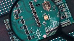
Such PCB tests can be applied to prototypes and small batches. They check boards for open short circuits and defect solder joints, as well as test their performance (Fig. 1). The same goals are pursued by testing in mass production.

Manufacturers use different methods for PCB and PCB assembly (PCBA) examination. The choice of testing approach is associated with the production scale, product characteristics, and novelty.
Let's take a look at the most used and well-known procedures.
Manual Vision Inspection
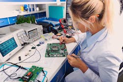
Manual visual inspection (MVI), the oldest method of PCB inspection, doesn’t require the use of expensive equipment (Fig. 2). Examination by a specialist can identify such visible defects as bad solder, lack of details or their wrong position, cracked joints, and interrupted traces.
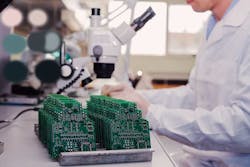
MVI isn’t a highly effective method for mass production due to human mistakes and the increasing complexity of boards with hidden joints. However, this approach works well in PCB design and small batch production.
Automated Optical Inspection
Automated optical inspection (AOI) is more suitable for large-scale production. An AOI machine compares the photo of the tested circuit board taken by a single 2D camera or two 3D cameras to the given example. This equipment may be placed at the end of the production line for timely flaw detection.
The AOI system can be effective as the first stage of PCBA testing. This method is more accurate than MVI, but AOI equipment needs a substantial amount of time to install and program for every PCB design change. That’s why it’s not a good option for prototyping.
AOI can be used together with other methods of PCB testing—e.g., with flying probes, in-circuit testing (ICT), or functional testing—for a more accurate and complete examination.
Automated X-Ray Inspection
Automated X-ray inspection (AXI) is a unique testing tool as it uses X-rays (Fig. 3). AXI creates 2D or 3D images of the hidden solder joints and can detect solder voids and open connections.

Being a rather costly and time-consuming technology, it’s best suited for mass PCB production and checking complex boards. It also can be rather useful for prototype design and small-batch testing, because it’s able to inspect the chip elements with pads that are out of sight.
In-Circuit Testing
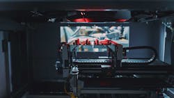
In-circuit testing (ICT), or a “bed of nails,” is a highly accurate type of electronics check (Fig. 4). This is a fully automated and expensive appliance, so ICT is preferable as a final testing stage of high-scale products with a design that doesn’t have to be changed.
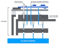
ICT powers up each component of the board and provides their automatic verification one by one for open short circuits and incorrect orientation, and checks resistance and capacitance, providing more than 90% fault coverage.
ICT equipment uses fixed probes (“nails”), which are set in correspondence with the PCB access points. Nails examine the integrity of solder joints and verify the undamaged connection. ICT test jig fixtures, which can be either mechanical or pneumatic, are very efficient for mass-production testing.
Another ICT advantage is that it can examine ball-grid-array (BGA) assemblies, FPGAs, and power up, as well as try out LEDs.
Flying Probe Testing
Flying probe electronics testing (FPT) is a more budgetary alternative to ICT—it doesn’t need a PCB test fixture and long programming time. However, testing PCBs with FPT is 15 times slower than ICT.
FPT appliance inspects a PCB with the help of probes; some of them are static (they’re under a tested PCB), others are movable (they ‘fly” over the board) (Fig. 5). The probes (“needles”) are programmed to check all components of PCB.
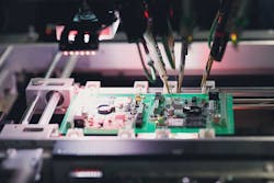
This method is more suitable for prototypes and not large batch production. It doesn’t need much space and much time for installation and provides a high percent of coverage, but is a bit slow in testing.
Stress Tests
Stress tests may be needed to evaluate the ability of circuit boards to endure maximum loads and parameter changes. The functioning conditions examined can involve temperature, current, operating frequency, or other significant parameters. These tests are specific and therefore can be used for certain types of PCBs.
Burn-in testing is a way to examine designed templates and PCBs for mass manufacturing (Fig. 6). Burn-in testing supplies power to the PCB, typically at its maximum-specified capacity for two to seven days. It aims to disclose any problems or defects of the board by using it in extreme or prolonged working conditions.

Stress tests are in the HALT/HASS (Highly Accelerated Life Testing/Highly Accelerated Stress Screening) group of methods. Their purpose is to determine and get rid of faults as well as guarantee the product’s quality at the development (HALT) phase or production (HASS) phase. They’re most often performed for printed boards used in specific applications—medical and industrial equipment, aerospace, and automotive vehicles. Stress tests can be done for newly launched products to ensure that they’re structurally and functionally reliable.
Functional Testing
The PCB Functional Test (FCT) examines the correctness of electronics performance (Fig. 7). These tests are usually carried out at the end of the manufacturing process to verify the functionality of the PCB and its compliance with the specifications.
Depending on the PCB design complexity, and consumer’s needs, tests may involve simply checking whether the board can be turned on or not, or a comprehensive full study.
PCB Laboratory Tests and Certification
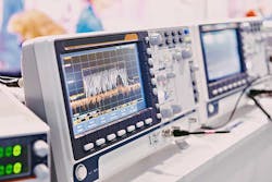
Specially equipped laboratories can thoroughly examine circuit boards (Fig. 8), using such appliances as an x-ray inner-layer registration tester, plating thick tester, impedance tester, copper adhesion tester, UV spectrophotometer, and many others.
Labs can confirm that the PCB meets all required requirements and specifications (Fig. 9).
Now let's take a look at some simulation tools in more detail.
Spice Simulation
Simulation Program with Integrated Circuit Emphasis (Spice) is a widely used simulation tool (Fig. 10). Different Spice software packages may have various functions, but almost all of them can do certain types of basic PCB analyses.
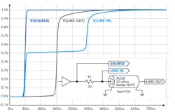
DC Operating Point Analysis works with static dc characteristics. It can calculate all dc performance in the datasheet.
The transient analysis works with the time response. It calculates the voltage and current for each period.
AC Analysis works with frequency characteristics. It calculates the small-signal response of a circuit board and gives simulation results such as gain and phase characteristics versus frequency.
Other SPICE tools, such as Temperature Sweep Analysis, Fourier Analysis, Noise Analysis, and Worst Case Analysis, also can be employed for a comprehensive investigation of PCB behavior.
IBIS Simulation
Input/Output Buffer Information Specification (IBIS), which simulates an integrated circuit’s input/output buffers, is kind of an alternative to Spice simulation (Fig. 11). It can be up to 100 times faster than Spice, but sometimes it’s less accurate. IBIS calculates the board’s behavior and can be used in PCB design at both schematic and layout steps.
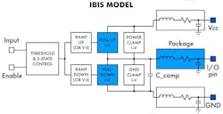
The key element of the IBIS model includes a table with current, voltage, and timing characteristics. The IBIS model doesn’t contain transistor-level data about the PCB, so vendors are assured about the safety of their intellectual property. Most IBIS models are easy to use and can be taken without restraint.
Conclusion
Testing is an essential stage of PCB design and production. Designers and manufacturers can choose and use appropriate investigation methods on their own or entrust them to special laboratories. Tests should guarantee the security and correct functionality of the PCB.
On that front, Integra Sources works with trusted and reputable manufacturers that conduct all required PCB tests. Nonetheless, our engineers pay a lot of attention to verifying all components of projects, running both hardware- and software-related tests.
About the Author

Andrey Solovev
Chief Technology Officer, Integra Sources
Andrey Solovev, CTO of Integra Sources, has 20 years of experience in the IT field. He possesses unique skills, as he has tremendous hands-on experience in electronics design and software development backed by fundamental knowledge of mathematics, physics, engineering, and programming.
Andrey has a Ph.D. in physics and mathematics. He has written over 20 scientific papers on automated spectral analysis, analog-digital converters, electro-optical diagnostics systems, and other topics. For 16 years, he has been a practicing university teacher. Andrey successfully combines technical management in the company with conducting university classes on system programming and robotics programming.
Under Andrey's technical guidance, Integra Sources has become one of the world's best development companies in various IT categories, according to prestigious research organizations.
Andrey often participates in IT meetings, exhibitions, seminars, and conferences, where he can share his rich experience in custom electronics design and software development and adopt the world's greatest achievements in this area.
Andrey takes an active part in editing and saturating the blog's articles with high-quality technical information.
Comment About the Article
To join the conversation, and become an exclusive member of Electronic Design, create an account today!

Leaders relevant to this article: