High-Performance Source for ADC and Audio Test with Novel DPD
Members can download this article in PDF format.
What you'll learn:
- What's required in a source for mixed-signal test.
- Key factors in achieving low distortion.
- Designing a signal-generation path.
- What is digital predistortion (DPD)?
- Using LDOs to power the test system.
The evolution of precision analog-to-digital converters (ADCs) and high-fidelity audio devices (codecs, MEMS microphones, etc.) continues to increase the demand for high-performance audio and arbitrary signal generation in automated test equipment (ATE). The multiple high-performance instruments required to characterize, validate, and test the dc and ac characteristics of these devices impose a premium on the cost of development and production test, with sometimes prohibitive or limiting test coverage.
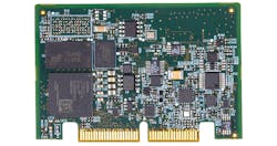
When possible, test engineers develop in-house solutions as an alternative, but this comes at the expense of time and resources. Reference designs such as the ADMX1002 ultra-low-distortion signal-generator module seek to offer an alternative to accelerate this development (Fig. 1).1
The ADMX1002 helps solve both the hardware and embedded software development challenges. In addition to abstracting the design complexity through a simple serial interface, it automates multiple sine-wave and arbitrary waveform generation. Moreover, with a novel digital-predistortion (DPD) algorithm, the reference design helps further improve the performance of the DAC and amplifiers in the signal chain.
High-Performance Mixed-Signal Test Needs
Modern ADCs and other mixed-signal devices often need a source to test high-performance dc and ac characteristics. In all cases, the source must exceed the performance of the device under test (DUT).
In terms of dc tests, they’re performed to guarantee that there are no missing codes and to verify differential nonlinearity (DNL), integral nonlinearity (INL), and offset and gain errors. These tests call for a low-noise and high-resolution dc-coupled, single-shot, linear signal such as a ramp to characterize the INL and DNL performance. For this type of test, high resolution is required to exercise all of the available codes in the ADC.
Specifications like total harmonic distortion (THD), signal-to-noise-and-distortion ratio (SINAD), and spurious free dynamic range (SFDR) are verified with ac tests. Such tests often are performed with a tone (sine wave) of the highest quality, which means it should not contain any harmonic content above the target specification.
To accomplish that task, test engineers can employ custom filters to eliminate undesired distortion products from their test signal, adding complexity and cost to their system. However, broadband noise coming from the source is difficult to filter around the signal of interest. This noise coming from the source must be below the noise floor of the ADC under test to ensure that it doesn’t degrade the desired measurement goals.
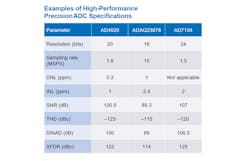
A summary of specifications published for high-performance ADCs is in the following datasheets: AD4020/AD4021/AD4022, ADAQ23878, and AD7134 as shown in the table. We can see that our goal is to have a THD that’s better than –123 dBc.
Key Design Considerations for Low Distortion: Resolution and Linearity
Distortion can be expressed as errors in the amplitude of a signal at any given point. These errors cause deviations from its ideal signal shape. For digitally synthesized signals, a true high-resolution DAC with linearity guaranteed down to the least significant bit (LSB) is key to accurately represent every sample of the signal of interest. Because INL and DNL are metrics that quantify a converter’s deviation from its ideal transfer function, these linearity errors have a direct impact on the reproduction of high-fidelity signals.
Because distortion of periodic signals is often expressed in terms of THD, we need to quantify the effect that resolution and INL have on THD to make the appropriate precision DAC selection. To observe low THD requires a low noise floor, which means high signal-to-noise ratio (SNR) is needed. Fundamentally, SNR of converters is limited by their quantization noise. It’s generally accepted that SNR and resolution are related by the expression:
where N is the number of bits available in the converter, fs is the sampling rate, and BW is the bandwidth of the measurement.2 From the table, we can see the need for an SNR that’s at least better than 100.5 dB or ideally 3X better, which is about 110 dB. Assuming a bandwidth up to the first Nyquist zone, the resolution required for 110 dB SNR is 18 bits.
Next, we need to quantify the relationship between INL and THD. For this, we assume a DAC with a weak second-order INL. Its transfer function can be expressed with the polynomial:
where y is the output of the DAC (in volts) and x is the input code. The first term’s coefficient a represents the ideal factor relating input code and output voltage. The second term represents the INL, and its coefficient b is much smaller than a. The generation of a cosine signal x(t) = cos(ωt) with this DAC will result in the output:
We can express the signal at the output of the DAC as:
The second term now shows second harmonic distortion (HD2). This relationship indicates that INL imposes a fundamental limit for the generation of low-distortion signals. This analysis also holds for higher-order INL terms, which generate higher-order harmonic-distortion components. For example, adding a third-order nonlinearity term of amplitude c results in a signal:3
Assuming we employ an 18-bit DAC (per our SNR calculation) with third-order INL of 2 LSBs, the distortion caused by the third harmonic can expected to be:
which would fall short from our design goal of better than –123 dBc. Adding two more bits will bring this distortion down by another 12 dB to –126 dBc. This means we need at least a DAC with 20-bit resolution to achieve our distortion goals.
Design of the Signal-Generation Path
The design of a source that can meet the distortion and noise requirements starts with a couple key components: the DAC and its voltage-reference circuit. This task can be achieved with the AD5791 20-bit precision DAC. Its high resolution and linearity of better than 1 LSB guarantee the most accurate reproduction of signal levels with errors smaller than 10 μV if a 10-V output range is used.
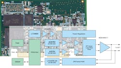
A simplified diagram of the output signal path is provided in Figure 2. Two AD5791s operate with opposite polarities to implement a fully differential path that further increases the SNR and decouples the signal of interest from ground-induced crosstalk. A low-noise voltage reference like the LTC6655, combined with the AD8676 precision op amp, provides the necessary positive and negative reference levels for high-linearity bipolar operation of each AD5791.
Because of AD5791’s high-precision architecture, a common challenge encountered when generating signals with precision DACs is the glitch energy generated between code transitions.4 Glitches distort the time-domain characteristics of the signal being generated, which deliver undesired amounts of energy to the DUT. For periodic signals, these glitches generate spurious content in the frequency domain that’s harmonically related to the fundamental tone.
A possible solution to this problem is to filter the glitch energy, which can drastically reduce the signal bandwidth and settling time of the source. A better solution is to implement a de-glitcher based on a sample-and-hold circuit5 with a low-charge-injection analog switch like the ADG1236 and the AD8676 op amp.
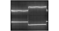
Figure 3 shows a 10-kHz square wave after (top) and before (bottom) the de-glitcher. The bottom trace shows the code transition glitch present at the output from AD5791. The DAC and de-glitcher update rate is 1 MHz. The residual charge injection from the switch isn’t harmonically related to the signal generated and can be easily filtered by the reconstruction filter at the output.
The resulting signals from the de-glitcher circuit are filtered before reaching the output with a multistage, sixth-order low-pass filter employing the ADA4945-1 fully differential amplifier (FDA). This high-order reconstruction filter is required to eliminate residual energy from the de-glitcher and images beyond the first Nyquist zone, which could alias back into the DUT’s input spectrum.6
The ADA4945-1 implements a differential output to meet the input requirements of modern ADCs. Moreover, each ADA4945-1 only contributes 1.8-nV/√Hz noise and achieves high precision with its guaranteed 0.5-μV/°C offset drift.
Digital Predistortion
Digital predistortion (DPD) is a technique used to minimize nonlinearities introduced by components on the path of a signal. DPD requires prior knowledge of the errors that need to be corrected so they can be subtracted from the signal during operation. Therefore, a measurement of the signal path must first be performed.
The challenge with measuring the signal path errors is that the measurement path needs to have lower distortion than the source path. Otherwise, the errors from the measurement path will be added to the source, thus degrading its performance. This isn’t easy to achieve, even with the best ADCs and amplifiers.
For example, the LTC2378-20, a 20-bit ADC with high intrinsic linearity, guarantees ±2-ppm INL, which is twice as much as the AD5791’s INL. This means that it’s not possible to measure the transfer function errors of the source path by simply digitizing multiple points of its transfer function. A better approach is needed.
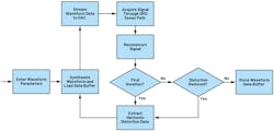
The ADMX1002 implements a patented DPD algorithm that improves the linearity of the measurement path used to correct source errors. Because the goal is to lower the distortion of sinusoidal waveforms, the source generates a single-frequency tone during the measurement phase. The DPD sense path preceding the ADC enhances the overall linearity of the path based on this type of signal.
Multiple digitized segments of the waveform are used to reconstruct the signal in the digital domain, which is then compared to a mathematical model. Correction parameters are extracted from this operation and applied to the generation of the sine wave. This process requires multiple iterations to null out random errors that could corrupt the result. Once the algorithm finds the optimal correction, it stops and stores the parameters used in the last iteration for signal generation. A simplified flowchart of the algorithm is shown in Figure 4.
Because the correction is specific to the signal being generated, this analysis must be performed for any other signal with different magnitude and frequency. To reduce the time required to set up different waveforms in an ATE system, the processed waveform data can be stored in an on-board flash memory and recalled at any time. The ADMX1002 can store up to 15 different waveforms, which also includes dual tones, or arbitrary patterns.
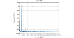
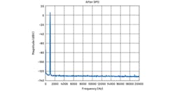
The distortion and noise performance of the signal chain without DPD is shown in the spectrum in Figure 5. The effect of the DPD algorithm on the same unit is revealed in Figure 6, with a total THD exceeding the –130 dBc mark. This is an improvement of 15 dB compared to the –115 dBc achieved by the hardware without DPD.
In addition to the DPD algorithm, an amplitude-correction algorithm uses the DPD sense path to compensate the attenuation that the reconstruction filter imposes on the source path.
Processing, interface, and control of the entire system are carried out by the system-on-chip (SoC), which includes FPGA fabric with an Arm core processor. The tasks carried out include:
- Waveform synthesis
- Predistortion algorithm execution
- Nonvolatile pattern memory management
- Precise timing control of the de-glitcher
- Data streaming to the DACs
- Control of the analog front-end switches
- Power-rail control and sequencing
- Host interface: SPI, status, parallel control
Additional DDR3 SDRAM supports the processing tasks of the SoC such as direct data streaming to the data converters.
Powering the System
When putting all of the pieces together, the hardware designer always faces the reality of bringing high-performance power rails to the entire system. The digital components often demand multiple low-voltage rails regulated at the point-of-load, while the analog and mixed-signal devices need to be properly decoupled from the power transitions of the digital components and powered with low-noise voltage rails. To simplify this task, instead of requiring multiple power rails to be generated, the ADMX1002 includes a power subsystem that consists of low-dropout (LDO) regulators and a power supervisor.
The LDO regulators eliminate unwanted ripple from upstream switch-mode power supplies, keeping the sensitive analog circuitry from picking up spurs that would otherwise be observed in the output spectrum. In addition, the critical power rails for the SoC are supervised by the LTC2962, which generates a power-good signal that can be polled by the host system for diagnostics.
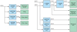
Overall, the ADMX1002 only requires three bulk power rails from the host: +3.3, +9.0, and –9.0 V. A simplified power tree is shown in Figure 7.
The task of generating low-noise ±9.0-V rails from a positive rail such as +12 V (common power rail in computer-based test systems) is a trivial task with the LTM8049, which doesn’t require external magnetic components or complicated layout. Likewise, stepping down the +12 V to +3.3 V can be achieved with the LTM8063.
Additional LDO regulators like the ADM7172-3.3, LT1965, and LT3015 can help guarantee that no ripple current flows into the tightly packed ADMX1002 to maintain a clean output spectrum. The block diagram in Figure 8 shows this configuration, which is employed in the EVAL-ADMX1002FMCZ evaluation board.
Conclusion
This article demonstrated that the demands for ADC and audio test can be met with a carefully designed signal path and signal-processing techniques. Achieving this goal requires high-resolution DACs, with attention to ensuring no glitches creep into the output, and implementing reconstruction filters with low distortion amplifiers.
Performance can be further improved with the implementation of a digital feedback path optimized with mixed-signal algorithms for accurate signal reconstruction. Moreover, a novel digital-predistortion algorithm can extract the harmonic distortion information that could be used to synthesize a waveform, which compensates the distortion of the source path.
References
1. Patrick Butler. “An Almost Pure DDS Sine Wave Tone Generator.” Analog Devices, Inc., December 2019.
2. Walt Kester. “MT-001 Tutorial: Taking the Mystery Out of the Infamous Formula, “SNR = 6.02 N + 1.76 dB,” and Why You Should Care.” Analog Devices, Inc., 2009.
3. Behzad Razavi. RF Microelectronics, Second Edition. September 2011.
4. Miguel Usach and Martina Mincica. “AN-1444 Application Note: Second-Order Effects to Consider for Continuous Precision DAC Updates.” Analog Devices, Inc., January 2017.
5. “MT-090 Tutorial: Sample-and-Hold Amplifiers.” Analog Devices, Inc., 2009.
6. “Why Does a DDS Need a Reconstruction Filter?” Analog Devices, Inc.
David Brandon and Ken Gentile. “AN-837: DDS-Based Clock Jitter Performance vs. DAC Reconstruction Filter Performance.” Analog Devices, Inc., December 2006.
Walt Kester. “MT-003 Tutorial: Understand SINAD, ENOB, SNR, THD, THD + N, and SFDR so You Don’t Get Lost in the Noise Floor.” Analog Devices, Inc., 2009.
Walt Kester. “MT-017 Tutorial: Oversampling Interpolating DACs.” Analog Devices, Inc., 2009.
About the Author
Gustavo Castro
System Applications Engineer, Analog Devices Inc.
Gustavo Castro is a system architect in the Instrumentation Business Unit in Wilmington, Mass. Prior to joining Analog Devices in 2011, he worked for 10 years designing high-performance digital multimeters and precision source-measurement units for automated test equipment at NI. He has contributed to several patents in the areas of analog, mixed-signal, and algorithm design for precision measurements and electronic instrumentation. Gustavo received his B.S. degree in electronic systems from Tecnológico de Monterrey and his M.S. degree in microsystems and materials from Northeastern University.
