IBIS Modeling (Part 1): Why IBIS Modeling is Critical to Design Success

This article is part of the Test & Measurement library series: Simulate Your Way to Design Success with IBIS Modeling.
Members can download this article in PDF format.
What you'll learn:
- What is IBIS?
- How to create IBIS models.
- Looking at the switching behavior of I/O buffers.
- Formatting the IBIS model.
- The two parts to the IBIS model validation process.
IBIS stands for input/output buffer information specification. It represents the characteristics or behavior of the digital pins of a device that IC vendors provide to their customers for use in high-speed design simulations. These models mimic the device’s I/O behavior using parameters specified by the IBIS Open Forum, an industry organization that manages and updates the specifications and standards for IBIS models.
IBIS models use an ASCII text file format by means of tabulated voltage-current and voltage-time information. They don’t contain proprietary data because the IC schematic design information—such as transistor sizes, parameters of the device model used in the design of the buffer schematic, and circuitry—aren’t revealed in the model. Furthermore, IBIS models are supported by most EDA vendors and can be run in a majority of industry-wide platforms.
Why Use IBIS Models?
Imagine an IC was tested, and it passed. And then a board was designed using that IC and subsequently endorsed immediately for fabrication. After the board was fabricated, the board performance failed and the failure was caused by some signal-integrity issues that resulted in crosstalk, overshoot/undershoot of a signal, or reflections caused by a mismatched impedance. What do you think happens next? Of course, the boards will have to be redesigned as well as refabricated.
At this point, time has been wasted and costs have risen—all because a very important stage was not performed: presimulation. This stage is where system designers use simulation models to verify the signal integrity of their design before building the board.
Simulation models such as Spice and IBIS are now being widely developed for use in simulations to help system designers foresee signal-integrity issues during the presimulation stage, so that they can be addressed before fabrication. This stage helps lessen the chances that the board fails during testing.
History
In the 1990s, with the rising popularity of personal computers, Intel started to develop a new I/O bus for its low-power ASICs operating up to around 33 MHz. There was a need to ensure that signal integrity wasn’t compromised, and this sparked the creation of IBIS.
A team led by Donald Telian came up with the idea of creating an information sheet for the I/O buffer and using this information in testing Intel’s boards. Soon it also shared these sheets with its customers for their board designs without giving any proprietary information. To be able to transfer the information from the paper-based spreadsheet reliably to the customer’s simulators, Intel decided to partner with EDA vendors and other computer manufacturers.
The IBIS Open Forum was created to help standardize a text-based machine-readable format of the buffer information. IBIS was originally called Intel buffer information sheet and later was changed to I/O buffer information specification. IBIS version 1.0 was issued in 1993.
From then on, the IBIS Open Forum continued to promote IBIS, provided tools and documentations, and improved the standard to add capabilities in specialized areas. In 2019, IBIS version 7.0 was ratified. This just goes to show that IBIS continues to advance and meet the new demands of technology.
How are IBIS Models Generated?
IBIS models generally model the device’s receiver and driver buffer behaviors without revealing proprietary process information. This is done by extracting the behavior of the standard IBIS buffer element and representing it through V-I and V-t data in tabular form.
In generating IBIS models, data gathering usually comes as the first step in the development process. Figure 1 shows the three main stages in generating IBIS models.
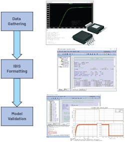
Data Gathering
There are two methods in gathering data for IBIS models:
- Simulation method: This method requires access to the design schematic of the part, the datasheet, and the lumped RLC package parasitics.
- Bench measurement method: This method requires actual units and/or eval board, the datasheet, and the lumped RLC package parasitics.
Figure 2 shows a diagram of the four main elements/components described in an IBIS model.
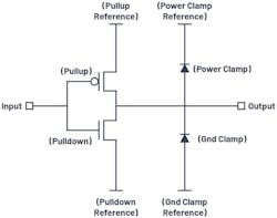
The two diodes connected to the pin are responsible for protecting the buffer in case the input exceeds the operating range or the buffer limit in terms of power clamp reference, which is typically VDD, and in terms of ground clamp reference, which is typically ground or –VDD, depending on how it was designed to operate. These diodes serve as ESD clamp protection and turn on as needed, whereas the pull-up and pull-down components are responsible for the driving the buffer’s behavior during high and low state. Thus, the pull-up and pull-down data are taken when the buffer is in operating mode.
These four main elements are represented in the model in the form of voltage vs. current (V-I) data, under keywords [Power Clamp], [GND Clamp], [Pullup], and [Pulldown]. The I/O buffer’s switching behaviors also are represented in the model in the form of voltage over time (V-t) data.
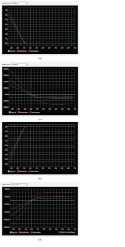
Voltage-Current Behavior Keywords
- [Power Clamp] represents the V-I behavior of the digital I/O pin’s power-clamp ESD protection diodes during high-impedance state, with respect to the power-clamp voltage reference.
- [GND Clamp] represents the V-I behavior of the digital I/O pin’s ground-clamp ESD protection diodes during high-impedance state, with respect to the ground-clamp voltage reference.
- [Pullup] represents the V-I behavior of the I/O buffer’s pull-up component when it’s driving high, with respect to the pull-up voltage reference.
- [Pulldown] represents the V-I behavior of the I/O buffer’s pull-down component when it’s driving low, with respect to the pull-down voltage reference.
The data for these keywords is taken in the recommended voltage range of –VDD to 2 × VDD, and in three different corners: typical, minimum, and maximum. The typical corner represents the behavior of the buffer when it’s operating in the nominal voltage, under nominal process and nominal temperature. The minimum corner represents the behavior of the buffer when it’s operating in the minimum voltage, weakest process, and highest operating junction temperature for CMOS/lowest operating junction temperature for BJT. The maximum corner represents the behavior of the buffer when it’s operating in the maximum voltage, strongest process, and lowest operating junction temperature for CMOS/highest operating junction temperature for BJT.
For each voltage swept in the pin, its corresponding current is measured, thereby gaining the voltage-current behavior required by the IBIS specifications in modeling the buffer. Waveform examples of these four V-I curves taken in three corners are shown in Figure 3.
Switching Behavior
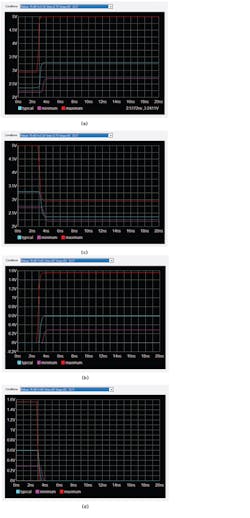
Aside from the V-I data, the I/O buffer’s switching behaviors in the form of rising (low-to-high output transition) and falling (high-to-low output transition) waveforms also are included in the V-t data table. This data is measured with a load connected to the output.
The load used is usually 50 Ω, to represent the typical transmission line characteristic impedance. It’s still best to use a load that the output buffer will actually drive. This load pertains to the transmission-line impedance to be used in a system. For example, if a system will use a 75-Ω trace or transmission line, then the recommended load to obtain V-t data is 75 Ω.
For a standard push/pull CMOS, four types of V-t data are recommended for inclusion in the IBIS model:
- Rising waveform with load referenced to VDD
- Rising waveform with load referenced to ground
- Falling waveform with load referenced to VDD
- Falling waveform with load referenced to ground
The two rising waveforms are contained under the model keyword [Rising Waveform]. It describes the low-to-high output transitions of the I/O buffer when its load is connected to VDD and ground, respectively. On the other hand, the two falling waveforms under the model keyword [Falling Waveform] describes the high-to-low transitions of the I/O buffer when its load also is connected to VDD and ground respectively.
It should be noted that because of the load connected at the output, it’s not expected that the output swings will make a full transition. Like the voltage-current behavior, the voltage-time data is taken in three different corners. Examples of these transitions are shown in Figure 4.
V-t tables also extract ramp-rate values. The ramp rate is the rate at which the voltage switches from one state to another, taken at 20% to 80% of the rising or falling transition edge. The ramp rate is listed in the IBIS model in the form of dV/dt ratio, under the [Ramp] keyword, which is normally shown after the V-t tables. This value is taken excluding the effects of the package parasitics, as it only represents the intrinsic output buffer’s rise-time and fall-time characteristics.
In addition, IBIS models include some of the datasheet specifications where the simulations are based, such as the operating voltage and temperature range, input logic voltage thresholds, timing test load values, buffer capacitance, and pin configurations. They also include the lumped RLC package parasitics. They can’t be found in the datasheet but are essential when simulating the traces for a high-speed design system, since these parasitics add loading effects to the simulations. They affect the integrity of the signal that passes through the transmission line.
IBIS Formatting
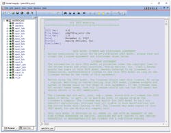
This section describes the second stage, which is building the model—also known as IBIS formatting. After gathering all necessary data, the model can now be created. An IBIS model consists of three main parts: the main header file, the component description, and the buffer model.
The main header contains the general information about the model (Fig. 5).
It specifies the following:
IBIS Version
- Model Keyword: [IBIS Ver]
- This is where the model is based. It tells the simulator’s parser checker what type of data to expect in the file; thus, it plays an important role in determining if the model passes the parser checker or not.
File Name
- Model Keyword: [File Name]
- This should present the actual name of the file, in lowercase format, using the proper file extension .ibs.
Revision Number
- Model Keyword: [File Rev]
- This helps track the revision level of the file.
Date
- Model Keyword: [Date]
- This shows when the model was created.
Notes
- Model Keyword: [Notes]
- This is included for the customer’s reference about the model—that is, if the data was taken from simulations or from bench measurement.
Source
- Model Keyword: [Source]
- This tells where the model originated or indicates the model provider.
Disclaimer
- Model Keyword: [Disclaimer]
Copyright
- Model Keyword: [Copyright]
Note that the first three items listed under the main header are required. Other items aren’t required but are good to include since they add additional details about the file.
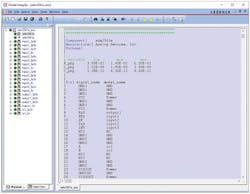
The second part of an IBIS model describes the component (Fig. 6).
For this part, the following data is required:
Component Name
- Model Keyword: [Component]
- As the name states, this is the name of the device being modeled.
Pin List
- Model Keyword: [Pin]
- This part appears in the model with at least three columns: pin number, pin name, and model name. This list is based on the datasheet. It should reflect the correct matching of pin number and pin name to avoid confusion. It also is important to note that in an IBIS model, each pin would have a dedicated model name. This model name may not necessarily be the same as the pin name stated in the datasheet because the pin’s model name is at the discretion of the model maker. In addition, some pins may point to one model name. This is the case for buffers having the same design schematic. It’s expected that they would have the same behavior, so one set of data is enough to represent them.
Manufacturer
- Model Keyword: [Manufacturer]
- It identifies the manufacturer of the component being modeled.
Package Parasitics
- Model Keyword: [Package]
- This item describes the electrical characteristics of the component’s package in terms of lumped resistance, inductance, and capacitance values. If the pin’s RLC parasitics also are available, it should be listed along with the pin list in the model under the [Pin] keyword. This provides a more accurate model and would override the RLC values listed under the [Package] keyword.
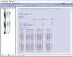
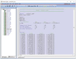
The third part of an IBIS model describes the buffer model. This is where the behavior of the I/O buffer is presented, particularly its I-V and V-t data. It begins by identifying the model name, using the [Model] keyword. The model name should match what’s listed in the third column under the [Pin] keyword.
For each buffer model, the parameter Model_type must be specified. Buffer capacitance also must appear under the parameter C_comp, to describe the capacitance seen when looking from the pad back to the buffer.
Types of Buffer Models
Different types of buffers can be modeled, and special rules apply for each. The following describes the four most common types of buffers and their requirements in an IBIS model:
Input Buffer Model Type: Input
This model type requires the values of input logic thresholds, under the parameters Vinl and Vinh (Fig. 7). If undefined, the default values to be used by the simulator are 0.8 V and 2 V, respectively. These parameters help the simulator perform timing calculations and detect signal-integrity violations.
Two-State Output Buffer Model Type: Output
This model type represents an output buffer that’s always enabled, either driving high or driving low (Fig. 8). It includes the timing test load values under the parameters Vref, Rref, Cref, and Vmeas. These parameters aren’t required, but their presence in the model will help the simulator in performing board-level timing calculations.
Note that since this type of buffer cannot be disabled, the keywords [Power Clamp Reference] and [GND Clamp Reference] will not be listed, as well as the V-I tabular data for [Power Clamp] and [GND Clamp].
Three-State Output Buffer Model Type: Three-State
This model type represents an output buffer that’s not only represented in its driving high and driving low state, but also in its high-impedance state, since this type of buffer can be disabled (Fig. 9). As with an output model type, it also includes the timing test load values under the parameters Vref, Rref, Cref, and Vmeas. Adding these in the model will help the simulator perform board-level timing calculations.

I/O Buffer Model Type: I/O
This model type is a combination of input and output buffer (Fig. 10). Therefore, the parameters to be included in this model are Vinl, Vinh, Vref, Rref, Cref, and Vmeas.
The model maker must take note of these guidelines in generating an IBIS model. More of these can be found in the IBIS Cookbook from the IBIS Open Forum website. Proper modeling guidelines must be followed; otherwise, a model will not pass the validation stage.
Model Validation
Validating an IBIS model is divided into two parts: the parser test and the correlation process.
Parser Test
When building the model, it’s best to use a software that already features a Golden Parser. This program performs the syntax checking and verifies data matching of the created IBIS model with reference to specifications of the model version. Some of the software with this feature are Cadence Model Integrity and Hyperlynx Visual IBIS Editor.
If the model passes the parser test, this means that the model generated follows the standard format and specifications, and V-I data matches with V-t data. If it doesn’t, it’s best to find out what causes the error. The simplest possible cause is there may be a format or keyword used in the model that wasn’t in accordance with the IBIS specification—this is easy and straightforward to correct.
The other type of error is the V-I and V-t data matching. When this occurs, it’s possible that the error lies in the pull-up or pull-down V-I data, or in the V-t data. This is the case where the behavior represented by the V-I data doesn’t match the behavior represented by the V-t data.
To address this issue, resimulation may be required. Before doing that, though, first review the voltage and loading values you’ve placed in the model and check if they’re correct. Save yourself from spending more time resimulating when the cause of error is as simple as a mistakenly defined voltage value.
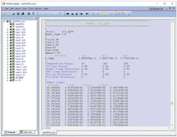
Figures 11 and 12 show, respectively, a sample IBIS model that failed and passed the parser test.
In Figure 11, observe how the software flags the error causing the model to fail during the parser test. This makes it easy for the model maker to correct the model before proceeding to the next validation step. In this example, the error is due to the model type used for the buffer. The IBIS specification requires the I/O model type to be entered in uppercase format, whereas in this figure, lowercase format is used.
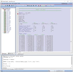
Figure 12 shows a model passing the parser test. Notice in the Model_type keyword that I/O was changed to uppercase format. This resolved the error.

A model can only proceed with the correlation process if it passes this stage.
Correlation Process
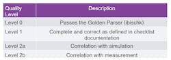
So, one might ask, how can we make sure that the generated model behaves as accurately as the actual part? The answer is the correlation process. There are different quality levels/correlations for IBIS models (see table).
This article describes a Quality Level 2a IBIS model. After passing the parser test, the model will be simulated, including the effects of RLC package parasitics with external loads added. The loads are typically the timing test load values found on the datasheets used in characterizing the I/O buffers. Similarly, the design schematic of the part will be simulated employing the same setup and loads. The results of both simulations will be superimposed to verify if the generated model matches the behavior of the schematic-based results. In another article, a use case on generating IBIS models will be presented using open-source software.
Why IBIS Models are Essential for Your Simulation
IBIS models are widely supported by most EDA vendors. They’re easy to use and come in smaller sizes, thus providing faster simulation time. They don’t contain proprietary process and circuit information, which enables most semiconductor vendors to readily provide IBIS models to their customers. And the models present all of these advantages while accurately modeling the device’s I/O behaviors.
IBIS models enable designers to foresee and address signal-integrity issues before proceeding to board prototyping or fabrication. Doing this puts them in a good position to shorten their board development cycles and, in turn, help speed up their time-to-market.
Simply put, customers use IBIS models because utilizing them in their simulations helps save not just cost, but also time in designing, debugging, and generating revenue from their board designs.
A collection of IBIS simulation models for Analog Devices’ products can be found here.
Read more articles in the Test & Measurement library series: Simulate Your Way to Design Success with IBIS Modeling.
References
Casamayor, Mercedes. AN-715—A First Approach to IBIS Models: What They Are and How They Are Generated. Analog Devices, Inc., 2004.
IBIS Modeling Cookbook for IBIS Version 4.0. IBIS Open Forum, September 2005.
IBIS Version 7.0. IBIS Open Forum, April 2020.
Leventhal, Roy, and Lynne Green. Semiconductor Modeling: For Simulating Signal, Power, and Electromagnetic Integrity. Springer, 2006.
About the Author
Jermaine Lim
Product Applications Engineer, Analog Devices Inc.
Jermaine Lim joined Analog Devices in October 2014 as a product applications engineer. Since then, her contribution to ADI has focused on developing IBIS models for various ADI products. Jermaine received her bachelor’s degree in electronics engineering from Pamantasan ng Lungsod ng Maynila.
Comment About the Article
To join the conversation, and become an exclusive member of Electronic Design, create an account today!

Leaders relevant to this article: