Contact-Free Wafer Testing Slashes Production Time, Cost
High testing parallelism can be achieved with contactless wafer testing, which leads to reduced production cycle times. It also eliminates the possibility of wafer damage during testing.
According to STMicroelectronics, it’s successfully tested dice on a semiconductor wafer without contact probes. Thus, electromagnetic waves can be used as the only link to test the array of circuits on a wafer.
The company believes a number of benefits are possible with this approach, including higher yields, shorter testing times, and lower product cost. In addition, contactless testing allows testing of RF circuits under conditions resembling real application conditions.
The new technology, dubbed ElectroMagnetic Wafer Sort (EMWS), was developed through an R&D project called UTAMCIC (UHF TAG Antenna Magnetically Coupled to Integrated Circuit), led by Alberto Pagani, Giovanni Girlando, and Alessandro Finocchiaro from STMicroelectronics, and Professor Giuseppe Palmisano from the University of Catania. The university won a prestigious “Sesames Award” in the “Production & Test” category at Cartes and IDentification 2010, held in Paris, France.
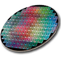
EMWS is an evolution of Electrical Wafer Sort (EWS), the last stage of wafer fabrication before assembly and test of the final packaged products. At this stage in the manufacturing cycle, the processed wafer contains an array of identical circuits. A probe card connected to automatic test equipment (ATE) is moved over each of the die and, in turn, the microscopic probes make contact with test pads on the die. The ATE then performs its tests to confirm that the die is fully functional, allowing any non-functional die to be discarded before die assembly and packaging.
With EMWS, the individual dice contain a tiny antenna. The ATE supplies power and communicates with the dice via electromagnetic waves. Such an approach reduces the number of test pads on the die. Though it still requires probes to supply power to test high-power products, ST’s technique enables fully contactless testing of low-power circuits.
ST says that contactless testing reduces the test cycle time because high testing parallelism can be achieved in contactless mode. Moreover, it increases yield by eliminating any potential pad damage during standard contact testing.
The contactless EMWS technology is based on a patented technique called electromagnetic concentration/expansion. It employs a passive structure consisting of two or more antennae connected together to obtain a series resonance that acts as an “electromagnetic lens.” The lens concentrates electromagnetic energy from a large surface onto a small one, such as a single die, or expands the energy from a small area to a larger one.
The Electromagnetic Concentrator/Expander, which can be incorporated into a testing system, helps increase the communication distance (reading range) between the die and an external system, such as the ATE, by at least one order of magnitude. Moreover, for ultra-low-power circuits like RFIDs, the concentrated electromagnetic energy can directly power the die, achieving fully contactless testing.
About the Author
Paul Whytock
Comment About the Article
To join the conversation, and become an exclusive member of Electronic Design, create an account today!

Leaders relevant to this article: