Get Acquainted with JTAG Basics
Download the PDF of this article.
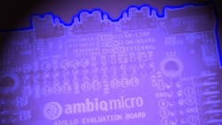
These days, hardware debug interfaces like the Joint Test Action Group (JTAG) IEEE 1149.1 standard are ubiquitous. You can find them on many microcontroller and microprocessor development boards, like Ambiq Micro’s Apollo (Fig. 1)—especially those targeted at developers or embedded systems. Most developers take these for granted and let hardware JTAG debug probes do the heavy lifting while using a debugger to deal with software problems.

1. The JTAG connector in the upper right provides hardware debug support for the ultra-low-power, Ambiq Micro Cortex-M4 Apollo microcontroller.
I was first introduced to boundary scan technology while working on a Burroughs B6700. This mainframe was built on wire wrap boards, required raised floor air conditioning, and had a boundary scan debug unit with hundreds of switches and lights that was the size of a refrigerator. A system with comparable computing power and storage fits in the palm of your hand, but the boundary scan approach remains the same. For those interested in Burroughs mainframes, check out the B5500 Emulation Project.
Texas Instruments’ (TI) SN74BCD8244 octal buffer (Fig. 2) highlights how boundary scan works. This harkens back almost all the way to those mainframe days. The Test Access Port (TAP) controls the scan chain within a device. The scan chain is essentially a giant shift register. Information is shifted in via the Test Data In (TDI) pin and out via the Test Data Out (TDO). This is synchronized with the Test Clock (TCLK), and the Test Mode Select (TMS) helps control the operation of the system. Commands and data are shifted in a bit at a time. This information can be loaded into the boundary control and instruction registers. The bypass register is a way to short-circuit the boundary scan register, as scan chains can be large and shifting through all the scan registers in a system can slow things down. When enabled, the bypass register adds a single bit to the chain.

2. The (obsolete) Texas Instruments SN74BCD8244 octal buffer was designed to be part of a JTAG scan chain.
When boundary scan was young, it was not uncommon to have truly unique implementations requiring matching debug tools. Luckily standardization has been pushing its way in so standards like IEEE 1149.1 and the newer 1149.7 allow standard JTAG probes like Segger’s J-Link Ultra+, IAR Systems’ I-jet Trace, and Macraigor Systems’ wifiDemon to work with a wide range of targets (Fig. 3). They all support the Boundary Scan Description Language (BSDL) that vendors use to describe the JTAG configuration of devices. BSDL is actually a subset of VHDL, the VHSIC Hardware Description Language.

3. Segger’s J-Link Ultra+ (left), IAR Systems’ I-jet Trace (center), and Macraigor Systems’ wifiDemon (right) provide JTAG connectivity using a range of host connections from USB to Wi-Fi.
The serial daisy chain approach allows multiple devices to be connected and supported by a single connector. A star topology is also possible and is needed for more complex designs. The IEEE 1149.7 defines six classes. Class T0 through T3 are extensions to IEEE 1149.1. Class T3 allows a star topology where devices are connected in parallel instead of serially. The devices are assigned unique ID codes so that only one device will be activated at a time. Class T4 and T5 implement an advanced two-pin operation. This reduces the pin out requirements but also limits bandwidth.
ARM microcontrollers and microprocessors are very popular. They support some alternatives when it comes to debugging, including the ARM Serial wire debug (SWD) interface and access to the on-chip ARM Instrumentation Trace Macrocell (ITM) and embedded trace module (ETM; Fig. 4).

4. ARM’s debug architecture includes the Instrumentation Trace Macrocell (ITM) and optionally the embedded trace module (ETM). The chips usually have a 10-pin JTAG interface or a 20-pin interface if ETM is supported.
SWD is typically used for microcontroller since it uses two or three signals, versus the four required by JTAG. The 10-pin Cortex header supports JTAG or SWD, although chips that support both will only work in one mode at a time. The 20-pin header is used when ETM is supported (see the table). Other JTAG pin configurations are possible.

These days, SWD and JTAG are often hidden behind USB-based microcontrollers that are on development boards along with the host processors. External JTAG probes are typically used on higher end platforms where performance is more important.
The IEEE P1687 Internal JTAG (IJTAG) standard was formalized in 2014. It uses the TAP but provides a more robust, hierarchical system designed to address the growing complexities of multicore system-on-chip (SoC) designs. It can support vendor-specific debug features and allow these to be hidden while allowing other features and conventional JTAG support to operate unfettered.

About the Author

William G. Wong
Senior Content Director - Electronic Design and Microwaves & RF
I am Editor of Electronic Design focusing on embedded, software, and systems. As Senior Content Director, I also manage Microwaves & RF and I work with a great team of editors to provide engineers, programmers, developers and technical managers with interesting and useful articles and videos on a regular basis. Check out our free newsletters to see the latest content.
You can send press releases for new products for possible coverage on the website. I am also interested in receiving contributed articles for publishing on our website. Use our template and send to me along with a signed release form.
Check out my blog, AltEmbedded on Electronic Design, as well as his latest articles on this site that are listed below.
You can visit my social media via these links:
- AltEmbedded on Electronic Design
- Bill Wong on Facebook
- @AltEmbedded on Twitter
- Bill Wong on LinkedIn
I earned a Bachelor of Electrical Engineering at the Georgia Institute of Technology and a Masters in Computer Science from Rutgers University. I still do a bit of programming using everything from C and C++ to Rust and Ada/SPARK. I do a bit of PHP programming for Drupal websites. I have posted a few Drupal modules.
I still get a hand on software and electronic hardware. Some of this can be found on our Kit Close-Up video series. You can also see me on many of our TechXchange Talk videos. I am interested in a range of projects from robotics to artificial intelligence.
Comment About the Article
To join the conversation, and become an exclusive member of Electronic Design, create an account today!

Leaders relevant to this article: