“Come on Feel the Noise”—Measuring LDO Performance
This file type includes high-resolution graphics and schematics when applicable.
With all due respect to heavy-metal band Quiet Riot (Fig. 1), who covered the song in the title (and the British band Slade who did the original 1973 version), if you can in fact “Feel the Noise” from your linear regulator, something is seriously wrong. Although seeing, smelling, or tasting the noise would arguably be worse!
In power-supply design, the linear regulator is widely used to tame the high-frequency transients emitted by high-efficiency switching supplies and prevent them from affecting sensitive analog and RF circuits. Unlike a switching topology, though, a linear regulator can only convert a higher input voltage into a lower output voltage—it includes a pass element that dissipates the excess power as heat. A low-dropout (LDO) design reduces the input-to-output voltage differential to 200 mV or less.
When specifying an LDO’s noise performance, we can distinguish between two types of noise, each one with its own datasheet parameter.
Internally Generated Noise
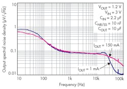
Intrinsic noise is generated in the device itself. It’s characterized by an output spectral-noise-density graph in the datasheet, which shows how the noise, expressed in μV/√Hz, varies over frequency. Datasheets typically include several graphs that describe how the output noise varies with output current (IOUT), output voltage (VOUT), and other parameters. Figure 2 shows the spectral-noise-density graph for the TPS7A49, an ultra-low-noise LDO designed for precision instrumentation applications.
Several different physical mechanisms contribute to intrinsic noise. Thermal noise results from the random motion of charge carriers (either electrons or holes) in a conductor; it’s proportional to absolute temperature and is independent of current flow. Thermal noise occurs in both active and passive devices; it’s one type of white noise and therefore has a flat spectrum.
Flicker noise, on the other hand, occurs only in active devices and varies by technology: PMOS vs. NMOS, for example. Flicker noise is proportional to current flow and inversely dependent on frequency; hence, its other name of 1/f noise.
Finally, shot noise is caused by electrons or holes randomly crossing a potential barrier such as a PN junction. It’s also associated with current flow and exhibits a flat frequency spectrum.
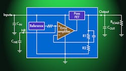
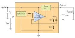
Although every block in the LDO shown in Figure 3 contributes to the overall output noise, the amplified reference noise forms the largest component because it has a large number of active and passive elements. In addition, any noise appearing on the reference is amplified by the error amplifier and has a disproportionate effect on the noise performance.
Externally Generated Noise and PSRR
The power-supply rejection ratio (PSRR), also called the power-supply ripple rejection, describes how well the LDO rejects noise from an external source that appears on its input. This external noise can originate from a switching power supply, parasitic coupling, or elsewhere. The PSRR compares the output ripple and the input ripple over the frequency range of interest for the application.
PSRR is expressed in decibels (dB)—the higher the number, the better the rejection. The equation is:
One of the dominant internal sources of PSRR in an LDO is, not surprisingly, the bandgap reference. Any ripple that couples from the input to the reference is amplified and appears on the output, so it’s important to have a bandgap reference with high PSRR.
Typically, the solution for both internal noise and PSRR is simply to filter the bandgap with a low-pass filter (LPF). As shown in Fig. 3, this LPF is accomplished by adding an external capacitor (CNR) to the existing internal resistor.
At low frequencies, the LPF reduces PSRR because it passes bandgap ripple in this range. A low-ESR ceramic output capacitor improves PSRR performance: The capacitance value should be chosen based on the frequencies that are important for the application. Finally, careful attention to board layout will reduce the feedthrough from input to output via board parasitics.
As an LDO’s load current increases, so does its open-loop output impedance, because the output impedance of its MOSFET pass element is inversely proportional to the drain current. This, in turn, lowers the gain. Increasing the load current also moves the output pole to higher frequencies, which boosts the feedback-loop bandwidth.
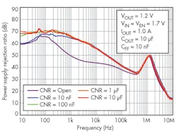
Increasing the load current, therefore, reduces PSRR at lower frequencies due to reduced gain, and increases it at higher frequencies due to more bandwidth. The TPS7A91 in Figure 4 includes circuitry to maintain a consistent PSRR over frequency. Its PSRR decreases by about 10 dB as the load current IOUT increases from 100 mA to 1 A, but this differential remains essentially the same from 1 kHz to 10 MHz.
For a deeper discussion of LDO noise, go here. PSRR is discussed in more detail here.
Measuring LDO Noise Performance
When characterizing an LDO and measuring its noise performance, it‘s important to ensure that the results reflect only the noise we’re interested in. We don’t want noise from the downstream power supply feeding the LDO to couple into the device and adversely affect the intrinsic noise measurement, for example.
As a result, each type of measurement has a different test setup and procedure.
Measuring Intrinsic Noise
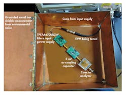
Figure 5 shows a typical test setup used to measure intrinsic noise. The LDO to be tested (the device under test, or DUT) is mounted on an evaluation module (EVM) and powered by an external power supply.
For lowest noise, a purely resistive load is used for the DUT. A battery is preferred as the power source, but this may not be practical for high-current DUTs. Bench power supplies are readily available, but tend to be noisy with spikes at the 50- or 60-Hz line frequency. A linear supply is preferable if available.
An LDO/filter block between the power supply and EVM helps to reduce the effects of power-supply noise. A passive pi-filter consisting of two capacitors and an inductor with a cutoff below the line frequency is one option, but will be expensive and bulky. Alternatively, an upstream LDO can cut down on power-supply noise while reducing cost and size. Make sure that it has low noise and high PSRR over a wide frequency range—for example, like those in the TPSA47xx ultra-low-noise LDO family.
A coupling capacitor after the DUT blocks its dc output and only passes the ac noise component to the downstream circuitry. Such a capacitor should have a 3-dB cutoff an order of magnitude lower than the lowest frequency being measured. This leads to a large-valued component when measuring frequencies down to 10 Hz, say, when used with a coaxial cable of 50-Ω characteristic impedance. The capacitor in Figure 6 is a parallel array of numerous smaller capacitors totaling 5100 μF. It’s housed in its own shielded box with coaxial connectors.
If the system noise floor is too high relative to the LDO’s noise output, an optional amplifier after the capacitor can boost the signal to help the spectrum analyzer more easily measure the signal.
The correct settings on the spectrum analyzer are also important. For example, the width of the bandpass filter (the resolution bandwidth, or RBW), should be at least a decade smaller than the measured frequency. This increases the resolution, but also extends measurement time.
The magnitude of the noise fluctuates due to its random nature: The averaging function makes multiple measurements of each point and averages the results. Set the sample average to between 25 and 50.
Finally, the whole test setup, shown in Fig. 6, should be mounted in a grounded and shielded enclosure to minimize the effects of environmental noise. For an in-depth discussion of the test setup and procedure, consult this application note.
Measuring PSRR
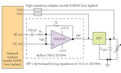
Figure 7 shows the recommended test setup to measure PSRR performance. The EB5061B Network analyzer generates both dc and an RF noise signal, then compares the input and output voltages to arrive at the results. The EB5061B has a frequency range from 5 Hz to 3 GHz.
A high-bandwidth amplifier acts as a summing node to amplify the analyzer output signal, provide isolation between the ac and dc components, and supply the DUT. The THS3120 is a low-noise, current-feedback amplifier that can provide an output current of up to 475 mA. The available EVM includes the required external components.
For best results, any LDO input capacitor should be removed before beginning the measurement, as a capacitive load could cause the high-speed amplifier to become unstable. To minimize added inductance, keep wire lengths as short as possible and use high-impedance probes placed directly on the VIN and VOUT pins to measure the input and output voltages.
While selecting the values of ac and dc inputs, be sure to keep within the specifications of the DUT. For example, the total input (VDC + VAC) to the DUT should be less than its absolute maximum input-voltage rating, and the value of (VDC – VAC) should always allow sufficient headroom (dropout voltage VDO) across the LDO at the specified output voltage.
At very high frequencies, the amplifier’s frequency response will roll off the ac component of the DUT input signal. Eventually, its effects will be too small to measure on the DUT output.
If a network analyzer isn’t available, an alternative approach uses a signal generator, a dc source, and an oscilloscope. With this setup, the PSRR graph is assembled piece-by-piece by calculating the PSRR at each ripple frequency and combining the results. This approach is obviously slow and cumbersome. Furthermore, the resolution and sensitivity of the oscilloscope at millivolt input levels limits it to LDOs with PSRRs of less than about 50 dB.
For further information on this topic, consult this application note.
Conclusion
LDOs are widely used to provide low-noise power in many sensitive analog and RF applications, and it’s important to be able to verify the LDO datasheet parameters in the lab. It’s just as important, though, that the test setup itself doesn’t skew the results. This article discusses some of the considerations needed to arrive at an accurate result.
About the Author
Paul Pickering
Paul Pickering has over 35 years of engineering and marketing experience, including stints in automotive electronics, precision analog, power semiconductors, flight simulation and robotics. Originally from the North-East of England, he has lived and worked in Europe, the US, and Japan. He has a B.Sc. (Hons) in Physics & Electronics from Royal Holloway College, University of London, and has done graduate work at Tulsa University. In his spare time, he plays and teaches the guitar in the Phoenix, Ariz. area
