Nanowire, Laser, Stimulated Emission Yield Tiny Refractive-Index Sensor

Most engineers are familiar with the basic physical parameters which need to be measured, such as temperature, pressure, position, velocity, and distance. But there are other key parameters which are critical as well. One such example is optical refractive index (RI), part of many liquid-based processes such as beer brewing, wine fermentation, assessment of water content in honey, and hydrocarbon distillation. There’s even a medical interest, since cancerous or abnormal cells tend to have a slightly higher RI value than normal ones.
The problem is that even miniaturized RI sensors—about the size of a coin—tend to be larger than many applications can accommodate. That’s what a team from the University of Michigan hopes to change by using the laser emission from a nanowire excited by an optical source. Its efforts are described in great detail, along with extensive references, in the paper “Refractive index sensing based on semiconductor nanowire lasers.”
At the core of the design in a 204-nm diameter, 15-μm long cadmium sulfide (CdS) wire that functions as an optical cavity (Fig. 1). The high refractive index of the nanowire causes impinging light to be reflected at the end facet with high reflectivity factor and guided along the nanowire. This arrangement forms a Fabry-Perot cavity which, in turn, is a source of lasing action when it is excited by an external light source. The resulting laser wavelength depends on the refractive index of its surroundings. By measuring the wavelength of the laser output, the refractive index of the liquid in which the nanowire is immersed can be determined.
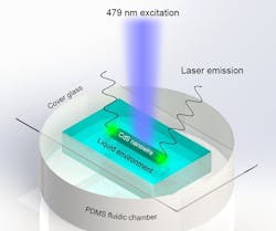
Fabrication uses a semiconductor-like process, with the CdS nanowire (refractive index n = 2.67) grown on a silicon-wafer substrate using a chemical-vapor transport process. The nanowires are next deposited directly on a silica cover glass, which is then exposed to low-pressure plasma. This plasma treatment is needed to ensure that the nanowire is immobilized on the glass surface, which is functioning for experiments in the liquid environment.
In tests, the nanowire was immersed in a mixed solution of ethanol and toluene with volume ratios of 10:0, 9:1, 8:2, and 7:3, corresponding to refractive indices of 1.365, 1.379, 1.393, and 1.407, respectively. The nanowire was excited by a pulsed optical parametric oscillator (5-ns pulse width, 20-Hz repetition rate, 479-nm wavelength). The pumping beam was focused using a 50× objective lens with a focal spot size of 60 µm. Figure 2 shows the resultant lasing spectra for each refractive index, all using the same excitation energy density of 4 µJ/mm2.
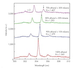
The tests also show that the wavelength effect is very sensitive. For example, there was a significant and measurable “red shift” from 504.35 nm to 505.23 nm when the refractive index increased from 1.365 to 1.407. Further analysis of the data, based on the 0.22-nm linewidth of the lasing peak and other factors, shows an overall figure of merit (FOM) of 96 for this design. Not only is this a 24× improvement over recently published results using a resonant-scattering approach, but the semiconductor nanowire sensor is less complicated to fabricate. It can be “internalized” into living cells and sense their individual refractive indices.

About the Author

Bill Schweber
Contributing Editor
Bill Schweber is an electronics engineer who has written three textbooks on electronic communications systems, as well as hundreds of technical articles, opinion columns, and product features. In past roles, he worked as a technical website manager for multiple topic-specific sites for EE Times, as well as both the Executive Editor and Analog Editor at EDN.
At Analog Devices Inc., Bill was in marketing communications (public relations). As a result, he has been on both sides of the technical PR function, presenting company products, stories, and messages to the media and also as the recipient of these.
Prior to the MarCom role at Analog, Bill was associate editor of their respected technical journal and worked in their product marketing and applications engineering groups. Before those roles, he was at Instron Corp., doing hands-on analog- and power-circuit design and systems integration for materials-testing machine controls.
Bill has an MSEE (Univ. of Mass) and BSEE (Columbia Univ.), is a Registered Professional Engineer, and holds an Advanced Class amateur radio license. He has also planned, written, and presented online courses on a variety of engineering topics, including MOSFET basics, ADC selection, and driving LEDs.
Comment About the Article
To join the conversation, and become an exclusive member of Electronic Design, create an account today!

Leaders relevant to this article: