When embarking on analog and power-supply designs, you will find yourself facing many decisions—from determining optimal operating parameters to choosing an effective circuit topology. Availing yourself of resources ranging from handbooks to training videos can help you get off to a smooth start.
A Look at Analog Designs
Members can download this article in PDF format.
One such resource is the latest issue of Texas Instruments’ Analog Design Journal, which describes circuits such as an ideal diode controller for solar applications. The controller works within a photovoltaic (PV) module-level power electronics (MLPE) optimizer.
A PV MLPE optimizer connects to an individual PV panel, as does a microinverter, and performs maximum power-point tracking (MPPT) for that panel as the panel experiences various illumination and shading conditions. Unlike the microinverter, the optimizer delivers not AC but rather regulated DC voltage to a string inverter, which then converts DC power from multiple panels into AC grid power.
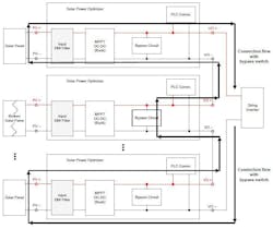
Optimizers exhibit drawbacks if not designed correctly. Figure 1 shows three optimizers connected to three solar panels. Unfortunately, though, the middle panel is faulty—a condition that could collapse the voltage of the entire string.
To enable the two good panels to continue providing voltage to the inverter, you can include a bypass circuit in each optimizer. Therefore, an optimizer connected to a damaged panel will not interrupt all power flow to the string inverter, as shown by the thick black arrows in Figure 1.
This bypass circuit can take several forms. A simple, low-cost approach is to use a diode, but the diode imposes a high forward-voltage drop, resulting in high power dissipation and heat. A more efficient solution is to use a MOSFET with low drain-source on-resistance.
With such an approach, however, the MOSFET requires a control signal, most likely from the MPPT controller. And that controller may depend on a functioning solar panel for power, rendering it inoperable when needed to activate the bypass switch.
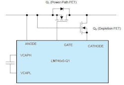
As a better solution, you can use a standalone MOSFET controller, such as a member of the TI LM74610-Q1 family of floating-gate ideal-diode controllers (Fig. 2). When the voltage at the device’s anode pin (VANODE) equals or exceeds the voltage at the cathode pin (VCATHODE), the power-path FET Q1 turns on, and the circuit operates in bypass mode. When the anode voltage is less than the cathode voltage, Q1 turns off, and the optimizer in which it’s used operates normally.
Adding the depletion-mode FET QD, operating as a source follower, enables the circuit to scale up in voltage from the 45-V rating of the LM74610-Q1 to 100 V or more. To add this bypass switch to an optimizer in Figure 1, connect the ANODE and CATHODE pins to the VO- and VO+ lines, respectively.
Power Tips for Converter Designs and More
Power supplies are critical to almost all analog designs. Even circuits that run on battery power may need buck or boost dc-dc converters to develop the proper voltages for the various components used in the design. TI’s Best of Power Tips eBook includes a variety of designs for efficient low-noise converters.
For example, one chapter describes flyback converters that operate either in continuous-conduction mode (CCM) or discontinuous-conduction mode (DCM), with the latter mode often proving to be the compact, lower-cost option for low-power applications. Figure 3 shows a simplified schematic of a converter that can operate in either mode, depending on the timing of the switching transistor Q1.
With DCM, the current through diode D1 returns to zero before each switching cycle, which minimizes losses in the transistor and diode as well as permits the use of a smaller, lower-cost transformer (T1). In general, DCM supports lower transformer primary inductance than CCM, with the inductance determining the maximum duty cycle. In addition, DCM eliminates rectifier reverse-recovery losses and minimizes FET turn-on losses.
DCM’s drawbacks include higher peak primary and rectifier currents, higher input and output capacitances, and potentially higher levels of electromagnetic interference.
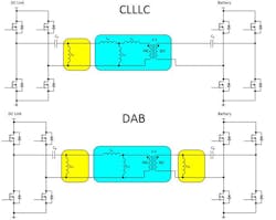
The eBook also presents a comparison of two circuit configurations for an electric-vehicle onboard charger (OBC): the capacitor-inductor-inductor-inductor-capacitor (CLLLC) and the dual-active-bridge (DAB) configurations, shown at the top and bottom, respectively, of Figure 4. Each has advantages and disadvantages. The DAB converter can provide higher levels of power over the entire output-voltage range, but it requires two commutation inductors (highlighted in yellow in Figure 4), whereas the CLLLC approach requires only one, thereby reducing weight.
In addition to the DCM and OBC designs, the eBook presents a complete 60-W CCM design as well as a half-bridge inductor-inductor-capacitor (LLC) series resonant converter for audio applications. In total, the book provides 25 tips on how to optimize your power designs.
Video Training Sessions
In addition to the journal and eBook, TI offers its TI Precision Labs comprehensive set of on-demand training videos. Analog topics include amplifiers, with separate videos addressing op amps, comparators, current-sense amplifiers, instrumentation amplifiers, and differential amplifiers. A section on sensors features videos focusing on temperature, magnetic, humidity, ambient-light, ultrasonic, and inductive measurements. Additional categories include motor drivers, switches and multiplexers, simulation tools, and data converters.
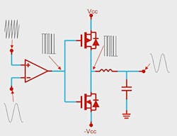
One video focuses specifically on amplifiers and data converters for audio applications, describing Class A, Class B, Class AB, and Class D amplifiers, such as push-pull transistors driven by a pulse-width-modulated (PWM) signal. Class D amplifiers (Fig. 5), often used in cellphones, tablets, and laptops, offer efficiencies to 90% with low audio distortion. TI offers class D amplifiers in its Smart Amps family of devices, which also include signal-processing and data-converter functionality.
Conclusion
Analog and power designs require careful preparation to ensure success. TI offers a range of resources, from journals and eBooks to videos, to start you on the right track.


