Boost AI Network Reliability with End-to-End 1.6T Interconnect Testing

What you'll learn:
- How interconnects become data center bottlenecks.
- Validating transceiver compliance at the physical layer.
- Checking signal integrity and cable testing.
- Scaling transceiver production without compromising quality.
- Going beyond physical-layer testing.
The “Era of AI” is here, transforming how we work and live, but it’s pushing data centers to their limits. Training large language models (LLMs) demands massive volumes of computing and memory, distributed across densely interconnected GPU clusters.
To keep up with model complexity and scale, hyperscale data center operators are racing to upgrade their networks to 800GE and 1.6T Ethernet. But boosting the network capacity with higher-bandwidth interconnects is only part of the story. The real challenge is how to boost interconnect reliability and efficiency to withstand the stress of continuous AI training workloads.
AI networks are only as fast as the weakest link between the clusters. Every transceiver, cable, and connector can affect system-wide throughput, latency, and reliability. Performance bottlenecks, interoperability gaps, and tail latency derail model training. As data center operators upgrade their networks to 1.6T networks and beyond, network architects must consider how each component performs under heavy AI workloads and real-world conditions.
Building to spec is just the beginning. Transceivers must be rigorously validated from design to manufacturing to ensure not just interoperability, but optimal system-level performance under real-world conditions.
This article explores the challenges of enabling 1.6T networks for AI data centers and highlights the best practices for validating device performance at the physical layer and beyond. You will gain a deeper understanding of the metrics that matter, the tools you need, and the strategies to help ensure your components are stress-tested and ready for deployment at AI scale.
How Interconnects Become Data Center Bottlenecks
Training LLMs isn’t just about raw compute power—it demands fast, synchronized communication across massive GPU clusters. These clusters are built with disaggregated servers connected through high-speed electrical and optical interconnects.
Training is broken down and processed in parallel across different cluster nodes, each node handling a portion of the model. All nodes must stay in lockstep to proceed efficiently (Fig. 1).

As workloads scale, so do the risks of imbalance. Parallelism creates a strong interdependence between nodes. Each node represents a potential weak link in the network. A single underperforming link, whether it’s a transceiver, cable, or switch, can bottleneck the entire cluster. In unoptimized networks, GPUs are left sitting idle over half the time, waiting on their next task due to slow interconnects.
To optimize AI workload processing, data center operators need to stress-test each component and interconnect in the network. Transceiver failures are a major cause of workload failures and tail latency, and almost 50% of training tasks fail from network or compute issues. This puts the onus on the transceiver and interconnect manufacturers to design not just for spec-sheet compliance, but also for high-margin performance in the high temperature and massive workload conditions commonly present in AI data centers.
Validating Transceiver Compliance at the Physical Layer
The first step to prevent your interconnect from becoming a bottleneck in an AI data center is physical-layer performance validation. During development, every 224-Gb/s electrical and optical lane must be rigorously tested for signal integrity, interoperability, and real-world reliability under stressed conditions representative of AI training workloads.
Electrical transmitter and receiver testing
1.6T transceivers must meet increasingly tight signal integrity and noise tolerance requirements for each of the 224-Gb/s electrical and optical lanes. Standards like the IEEE P802.3dj for 1.6T Ethernet specify limits for transmitter jitter, transmitter dispersion penalties, bit error rate, and signal-to-noise-and-distortion ratio.
On top of that, real-world workloads in AI data centers push devices far beyond normal operational limits. Ensuring performance margins under increasingly strict physical-layer specifications is difficult, but important for device reliability and interoperability.
Signal integrity is paramount for electrical testing. Key transmitter measurements include jitter, signal-to-noise-and-distortion ratio, linearity, and signal-to-residual-intersymbol-interference ratio. Characterizing and tuning equalization on the transmitter for the best, clearest transmission is key to compensating for channel loss.
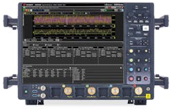
Developers need a high-bandwidth oscilloscope for signal capture and analysis (Fig. 2). Conformance automation software can guide users through complex validation needs and tests that determine pass/fail status for each required specification. Further signal-integrity and debugging software can help solve challenging conformance issues.
Receiver testing involves using a bit-error-rate tester (BERT) to inject stressed patterns and quantify error rates under degraded conditions. This is necessary for compliance testing, but it’s especially vital for linear pluggable optics (LPO), a new transceiver topology that sacrifices a DSP to reduce its power consumption. This significantly reduces the performance margin for the network interface card and switch, where the host chip must accommodate for a much more distorted and noisier signal.
Picking the right BERT and oscilloscope to perform this testing is a matter of choosing a pattern generator and error detector that use the right modulation format and correct symbol rate (120-Gbaud PAM4 for 224-Gb/s signals).
Optical transmitter testing
Testing optical performance is all about making accurate transmitter dispersion and eye closure quaternary (TDECQ) measurements. TDECQ quantifies the power penalty introduced by a real transmitter compared to an ideal reference at a specific target symbol error rate (SER). It aggregates impairments such as bandwidth limitations, noise, and inter-symbol interference in a single metric.
Ethernet standards rely on TDECQ as the primary metric for testing optical transceivers as a pass/fail criteria for compliance, so it’s a key differentiator for transceiver reliability and interoperability.
>>Download the PDF of this article, and check out the TechXchange for similar articles


Other important optical metrics include optical modulation amplitude (OMA—the optical power gap between optical 0 and 1 levels), extinction ratio (the ratio of power between high and low logic levels for laser performance), reference equalizer noise enhancement coefficient (Ceq), and laser relative intensity noise (RIN).
Optical measurements are typically made with a low-noise sampling oscilloscope. An ideal sampling oscilloscope for 224-Gb/s validation has extremely low intrinsic noise (<20 µW RMS) and jitter (<90 fs RMS) for the best optical accuracy and sensitivity. 112-Gbaud clock recovery is also required for compliance with 224-Gb/s optical measurements (Fig. 3).
Automated test programs integrate with oscilloscopes to perform quick TDECQ for compliance validation. Sampling oscilloscopes can be used to evaluate device performance both during R&D and manufacturing, characterizing waveform quality, analyzing impairments, and allowing for fine-tuning of equalization.
The higher the optical sensitivity, the more measurement margin you can achieve, giving you a better characterization of the device’s signal-integrity performance. Margin testing with stressed eye conditions over various temperature variations is key to ensuring more robust operation in real-world conditions.
Checking Signal Integrity and Cable Testing
Transceivers are only as good as the interconnects and cables that carry their signals. While most AI data centers rely on optical links today, some deploy active copper cables (ACCs) or traditional passive copper cables.
Regardless of the medium, ensuring robust signal integrity at 224 Gb/s is challenging: channel loss budgets are higher, reflections are more disruptive, and crosstalk more intense. Small discontinuities or impedance mismatches can significantly degrade performance. Characterizing and analyzing this behavior requires advanced measurement techniques.
S-parameters analysis gives a frequency-domain view of insertion loss (signal power lost along the channel), return loss (reflections due to impedance mismatches), and crosstalk (unwanted coupling between adjacent signal paths). Characterizing S-parameters for 224-Gb/s links requires a vector network analyzer (VNA) supporting 70- to 110-GHz bandwidth. Channel operating margin (COM) is a threshold metric included in recent IEEE 802.3 specs that combines insertion loss, reflections, crosstalk, and noise.
Time-domain reflectometry (TDR) complements frequency-domain analysis by adding spatial resolution, revealing the location and magnitude of impedance mismatches in complex PCB traces, connectors, and cables. Many modern VNAs and high-speed oscilloscopes now include TDR modes to isolate root causes of discontinuities.
Finally, de-embedding is essential to remove the effects of test fixtures and adapters from the measurement path, ensuring that measurements reflect only the behavior of the device under test (DUT). This improves simulation correlation and measurement accuracy. A popular algorithm for accurate de-embedding of physical structures within high-speed digital channels is Automatic Fixture Removal (AFR).
Scaling Transceiver Production Without Compromising Quality
Once a transceiver design is finalized, manufacturers need to ramp up volume production quickly to meet AI data center hardware demands. Slow manufacturing ramps can mean missing the market entirely, but manufacturers also can’t cut corners. It’s critical to maintain high yields to avoid shipping faulty units and causing problems in final deployment. The challenge for QA engineers is to ramp production quickly without compromising reliability or test accuracy.
Many test engineers build their test programs around sampling oscilloscopes, using them to “tune” their optical transceivers during manufacturing. In a fast feedback loop, the production system writes initial settings into a newly built transceiver module (such as laser bias, modulator voltage, etc.), then immediately measures a key performance metric like TDECQ.
Based on the measured result, the settings are adjusted, and the metric is measured again. This loop repeats rapidly until the transmitter is optimized and the device can pass performance thresholds.
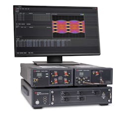
Typically, optimization testing is performed at multiple temperature setpoints as well, ensuring that each unit will perform optimally across the device’s entire operating temperature range. The sampling oscilloscope can be paired with an optical switch and test automation software to facilitate testing each lane, enabling testing multiple lanes and devices at once to reduce test time and improve hardware utilization (Fig. 4).
Going Beyond Physical-Layer Testing
Meeting physical-layer compliance is necessary, but it’s only the beginning for ensuring transceiver performance in AI data centers. Standards like IEEE 802.3dj define specifications at 224 Gb/s per lane, but many issues can crop up in real-world conditions that aren’t detectable from physical validation. As links approach and expand beyond 1.6T speeds, you need to take testing to the next level by stress testing beyond the physical layer.
“Layer 1.5”: Forward Error Correction
At these speeds, forward error correction (FEC) is essential to keep the aggregate bit error rate (BER) at an acceptable level across all lanes for reliable data transmission. While receiver compliance tests focus on pre-FEC BER, a compliant receiver still needs to perform at an acceptable BER level for FEC to be effective. Post-FEC analysis is about determining the error distribution where FEC becomes unreliable. Even with an average BER within spec, burst errors can exceed FEC limits and lead to unrecoverable frame loss.
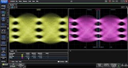
Because AI data centers demand near-zero data loss, FEC performance is crucial to analyze. That’s why analyzing post-FEC performance, specifically error distribution and frame loss rate (FLR), is just as important as traditional receiver compliance metrics. Interconnect test platforms can stress devices under full 1.6T loads using real packet flows and impairments to simulate system-level noise and congestion.
By validating end-to-end link behavior, including FEC tail analysis to examine how a receiver handles consecutive errors, developers can assess whether a transceiver is truly ready for AI deployment (Fig. 5).
Layers 2-3: Network Performance Testing
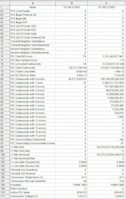
For AI data center transceivers, testing can’t stop at Layer 1. It’s critical to extend validation to full protocol stack performance. Developers should validate Layer 2/3 behavior under realistic conditions to uncover issues related to MAC addressing, routing, IP packet handling, and transport efficiency, ensuring that transceivers can support parallel data transfers of AI training workloads.
Emulating real Ethernet/IP traffic patterns at full line rate can expose issues in routing, flow control, latency, link stability, and congestion that aren’t visible through physical waveform analysis alone (Fig. 6).
Combining physical-layer validation, FEC-aware receiver testing, and full protocol stack (Layers 1-3) emulation, transceivers developers can have a more complete picture of transceiver performance. This holistic approach may seem like a lot, but it’s critical to ensure the reliability, throughput, and efficiency of AI data center interconnects as networks upgrade to 1.6T Ethernet and beyond.
What’s Next? Early Pathfinding and R&D
As the industry prepared to deploy 1.6T Ethernet over 224-Gb/s lanes, some developers are already looking toward the future. The next step, the technological jump that will push data center speeds to 3.2T Ethernet, is 448-Gb/s lanes.
Three primary signaling options are under evaluation: 224-Gbaud PAM4, 174-Gbaud PAM6, and 150-Gbaud PAM8. Each presents tradeoffs in complexity, bandwidth, and noise tolerance. Early research shows that any of these potential methods could be valid, and some developers are already working to find the best solution using high-speed arbitrary waveform generators and sampling oscilloscopes.
At the same time, emerging transceiver topologies like LPO, enabled by new photonic ICs, may affect these choices as performance demands and priorities change and reshape the next generation of data standards.
Interconnects are No Longer Just Passive Links that Require Advanced Testing
Regardless of the direction taken by the next generation of data standards, one thing is clear: Interconnects are no longer just passive links in the system—they’re critical performance enablers. In the new AI data center architecture, every component, transceiver, and interconnect is a potential weak link. Developers and architects must shift their mindset beyond interoperability compliance to performance optimization at every level.
It's a large task to take on, but with advanced end-to-end test, automation, and emulation tools from forward-looking companies like Keysight, every step in the design and validation cycle is achievable, and every improvement can have an outsized impact on efficient, reliable AI data center operations.
>>Download the PDF of this article, and check out the TechXchange for similar articles
About the Author
Ben Miller
Product Marketing Manager, Digital Products, Keysight Technologies
Ben Miller is Product Marketing Manager of Digital Products at Keysight Technologies.
Comment About the Article
To join the conversation, and become an exclusive member of Electronic Design, create an account today!

Leaders relevant to this article: