Demonstrating the Popular NEC Infrared Protocol
What you'll learn:
- How to implement NEC protocol logic on a configurable mixed-signal IC.
- Discover ways to eliminate external components and reduce coding complexity.
- Configure up to nine custom commands using the Memory Table Configurator.
- Verify NEC compliance through captured waveform analysis.
- Explore practical validation using Arduino UNO and a Keyestudio IR Receiver.

The NEC protocol is one of the most widely used standards for infrared (IR) communication in home automation applications like television remotes. It’s known for its robust and straightforward pulse-distance encoding scheme.
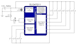
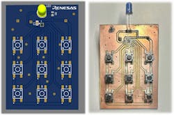
This article demonstrates how the Renesas SLG47011 can implement NEC protocol control logic efficiently by leveraging its built-in resources, eliminating the need for external components or complex microcontroller code (Fig. 1). The SLG47011’s configurable architecture supports up to nine user-defined commands through the Memory Table Configurator, making it adaptable for a range of IR remote-control applications.
The NEC Infrared Transmission Protocol
Since the NEC protocol utilizes pulse distance encoding, it’s important to remember how logical bits are transmitted to program a custom message (Fig. 2).
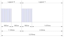
Here’s the timing for a pulse:
- Logical ‘0’ – a 562.5-μs pulse burst followed by a 562.5-μs space. Total transmit time is 1.125 ms.
- Logical ‘1’ – a 562.5-μs pulse burst followed by a 1.6875-ms space (3 × 562.5-μs intervals). Total transmit time is 2.25 ms.
Looking at the design in Figure 1, NMOS OD PINs 4-5 are connected in parallel to increase output signal current. As such, the waveforms will show you an inverted version of the output signal.
According to the NEC protocol specifications, a standard carrier frequency of 38.222 kHz is used. In this design, a frequency of 38.167 kHz was chosen as the closest match to the specifications.
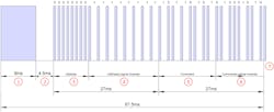
The structure of the NEC protocol message is defined as follows:
- 9-ms leading pulse burst (16 times the pulse burst length used for a logical data bit)
- 4.5-ms space
- 8-bit address for the receiving device
- 8-bit logical inverse of the address
- 8-bit command
- 8-bit logical inverse of the command
- Final 562.5-µs pulse burst to signify the end of message transmission
The NEC protocol message structure sends address and command data and its inverse in each packet (Fig. 3). The message is sent when a key is pressed.
If a key remains pressed, a repeat code will be sent every 110 ms (Fig. 4). The repeat code is 9 ms followed by a 2.25-ms space and a 560-µs burst.
Although the NEC protocol has a standard message structure, the extended version of it is frequently used. In the extended version of the NEC protocol, to increase the range of possible addresses, instead of including the 8-bit logical inverse of the address, the second frame represents a register address. This design is developed with the extended NEC protocol in mind.
A GreenPAK NEC Protocol Design
GreenPAK is a family of programmable, mixed-signal chips from Renesas. In this example, the design (Fig. 5) consists of five main phases:
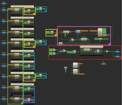
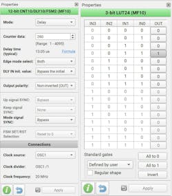
1. The first phase involves detection of the input signals. To ensure proper functionality of the design, each input signal is connected to a CNT/DLY block that serves as a deglitch. The deglitch delay time is configured to be 40 ms on a rising edge of the input signal.
2. During the second phase, the design checks whether only one input signal is at a high level. In this scenario, 3-bit LUT4 switches from its idle state, high to low, which resets the Memory Control Counter.
>>Download the PDF of this article

3. The third phase of the design is responsible for the NEC protocol control logic. The Memory Table block paired with the Width Converter (in 12 to 12 mode) is used to manually set the desired commands (including RepeatCode):
- OUT0-OUT8 contains nine possible messages.
- OUT10-OUT11 contains the RepeatCode and the RepeatEnable signals respectively (RepeatEnable is a custom signal that switches from idle state, low to high level, 40 ms after the end of a message).
- The Width Converter block utilizes an internal clock signal with a period that corresponds to 1.778 kHz to ensure that the length of each bit is 562.5 µs.
- The DFF block is used as a one-bit memory cell. The DFF block resets every time a single input signal switches to a high level; it will pass the RepeatCode signal to the output bus only when the input signal is kept high for more than 108 ms.
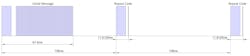
While setting up custom messages, it’s important to remember the main operating principles of the Memory Table block. The Memory Table block can hold and send out up to 4,096 12-bit words. Each word requires two bytes to hold, with the last four bits left unused. In the Memory Table’s Manual Editor mode, you can see that each 12-bit word is stored in parallel between 12 outputs (OUT0(LSB) - OUT11(MSB)) so that each OUT is responsible for holding one of the 12 bits of that word.
For example, to receive a message 10011100 (LSB) on OUT0, the following steps should be taken:
- Split the desired message into two chunks.
- Swap them.
- Mirror each of those chunks horizontally.
- Write down the hex value of the resulting combination in the Memory Table (Fig. 6).
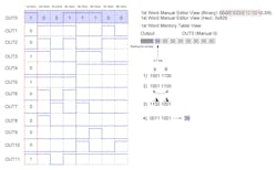
Alternatively, the Manual Editor can be used to set up the 1st through 8th word manually.
4. The fourth phase of the design serves as a 3-bit multiplexer for each message on OUT0-OUT8, which allows the command to pass through only when the RepeatEnable signal is low.
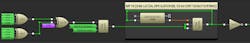
5. The fifth phase of the design serves as the main BUS for all signals (Fig. 7).
Afterwards, the passing signal is modulated with a 38.222-kHz frequency generated by the internal clock as shown in the MF10 block (Fig. 8).
As mentioned previously, the output signal is passed through an inverter to drive the IR LED through the OD NMOS.
Using the NEC Protocol Control Logic Demonstration Board
A demonstration board (Fig. 9) was created to test the viability of the design.
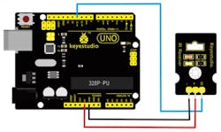
To decode the NEC protocol, an Arduino UNO and a Keyestudio IR Receiver were used in testing the design. Figure 10 shows these devices along with the connections used.
The following source code was used on the Arduino UNO board:
#include <IRremote.h>
// You may change PIN number according to your needs.
const int IR_RECEIVE_PIN = 11;

void setup() {
  Serial.begin(9600);

  IrReceiver.begin(IR_RECEIVE_PIN, ENABLE_LED_FEEDBACK);
}
void loop() {

  if (IrReceiver.decode()) {

    Serial.println("========================================");
    Serial.print("Protocol: ");
    Serial.println(getProtocolString(IrReceiver.decodedIRData.protocol));

    Serial.print("Data: 0x");
    Serial.println(IrReceiver.decodedIRData.decodedRawData, HEX);

    if (IrReceiver.decodedIRData.flags & IRDATA_FLAGS_IS_REPEAT) {
      Serial.println("Repeat Code (Key is kept pressed)");
    }
    Serial.println("========================================");
    Serial.println();
    IrReceiver.resume();
  }
}
The “Data” fully matches the programmed command through the MemoryTable block (LSB first).
Test Results
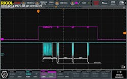
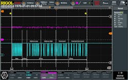
The design was tested in hardware and the following waveform results were obtained. The channels on each figure are:
- CH3 (pink): Active-high input signal
- CH2 (blue): Modulated output signal
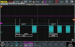
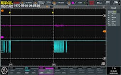
Figure 11 shows the modulated output signal covering the initial message and repeat code obtained on the demonstration board.
The initial message timeframe measured via Cursor tools confirms that the message transmission timing complies with the NEC protocol specification (Fig. 12).
Logical ‘1’ and ‘0’ standardized timeframes are shown to be further confirmed via the Cursor measuring tool (Fig. 13). Part of the initial message frame is depicted.
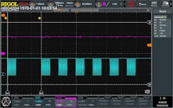
The waveform shown in Figure 14 demonstrates logical ‘1’ and ‘0’ timeframes.
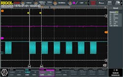
In Figure 15, the waveform demonstrates a logical ‘1’ timeframe. The measurements were carried out via the Cursor tool.
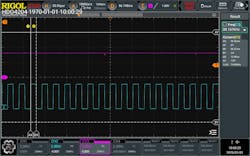
The waveform in Figure 16 demonstrates carrier frequency. The measurements were carried out via Cursor and oscilloscope measure tools.
In Figure 17, the waveform demonstrates the RepeatCode timeframe. The measurements were carried out via the Cursor tool.
Conclusion: Achieving NEC Protocol Compliance
The captured waveforms clearly verify compliance with NEC protocol specifications, confirming the design’s accuracy and reliability. The solution successfully transmitted commands to a receiver without error. Practical validation was carried out using an Arduino UNO platform paired with a Keyestudio IR Receiver, demonstrating the design’s robustness and readiness for real-world IR applications.
For related documents and software, visit:
Download the free Go Configure Software Hub to open the design file and view the proposed circuit design. Use the GreenPAK development tools to freeze the design into your own customized IC in a matter of minutes. See a complete library of application notes featuring design examples, as well as explanations of features and blocks within the Renesas IC.
>>Download the PDF of this article
About the Author

Oleksandr Lykhanskyi
Computer Science Student, Ukrainian Catholic University, and Renesas
Oleksandr Lykhanskyi is a sophomore Computer Science student at Ukrainian Catholic University specializing in Robotics. Passionate about electronics and embedded systems, I aim to deepen my knowledge in a field of UAV autonomous navigation.
Comment About the Article
To join the conversation, and become an exclusive member of Electronic Design, create an account today!

Leaders relevant to this article: