Rad-Hard-by-Design: GaN Semis for Next-Gen Space and Defense Systems
What you'll learn:
- Why GaN components are highly resistant to radiation damage, such as total ionizing dose (TID), making GaN well-suited for harsh space environments.
- Why GaN devices remain vulnerable to single-event effects (SEEs) and require careful system-level design.

Spacecraft must have radiation-hardened (rad-hard) electronics on board simply because radiation can cause electronic equipment to malfunction. Thus, power-management devices are critical for powering all of the electronics on board satellites and spacecraft, especially when astronauts are present within the spacecraft.
For instance, deep-space missions will likely encounter neutrons from background radiation or radioisotope thermal generators (RTGs), as well as other harmful nuclear sources (Fig. 1). And terrestrial and atmospheric environments may be exposed to galactic cosmic rays (GCRs) along with secondary emissions.
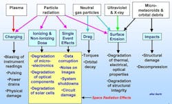
Moreover, long-term radiation effects in space can affect astronauts and spacecraft electronics. Total ionizing dose (TID) levels, which will be received at the component die level, are calculated for active parts while taking into account the spacecraft's defensive shielding. Protons and electrons will typically lead to a cumulation of long-term damage in space.
Called displacement damage (DD), it will cause extensive non-ionizing damage (this is usually not applicable to CMOS microelectronics). Transient effects can be affected by single-charged particle effects (single-event effects or SEEs) along with hard (destructive) or soft errors.
Why “Radiation-Hardened by Design” is Important
Designers can combat such damage with a radiation-hardened by design (RHBD) method, which will help meet performance, cost, and availability needs. Consequently, demand is great for high-performance semiconductors in real-time imaging applications among the space and defense sectors. However, the availability of components is quite limited, creating challenges within the RHBD industry.
This, coupled with high radiation-tolerant electronics larger than 1 milligray (MGy), a unit of absorbed radiation equivalent to one thousandth of a gray, or 0.1 rad for nuclear fusion and small modular reactors (SMRs), is restricted due to performance and limited availability.
>>Download the PDF of this article

There are now two solutions to utilize electronic components in harsh (radiation-filled) environments:
- Upscreening of commercial off-the-shelf (COTS) components.
- Use of space-grade radiation-hardened electronics.
RHBD is a door-opener to applications that require extremely high-dose-tolerant ICs and meet the demanding reliability and electronic performance guidelines of the space and military industries.
Rad-Hard GaN Wide-Bandgap Power Semiconductors
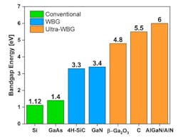
Some people think that wide-bandgap (WBG) semiconductors are naturally radiation-hard. However, the “inherent” radiation hardness of WBG semiconductors typically refers to their tolerance of total dose. The total dose for WBG semiconductors (Fig. 2) refers to their tolerance to radiation, specifically their ability to withstand ionizing radiation without significant degradation.
Radiation hardness assurance (RHA) is defined as the activities undertaken to ensure that the electronics and materials in a space system can perform to the design specifications after exposure to the natural space radiation environment.
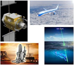
Spacecraft, along with some key avionic power systems, include lunar and planetary surface power, Mars transport and lunar gateway, small fission reactors, small satellites, and electric aircraft. Scientific payloads and instruments, such as LiDAR and mass spectrometers (Fig. 3), are also included.
GaN WBG Technology: Size, Weight, and Power (SWaP)
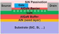
GaN has a fast-switching superjunction technology with voltages under 650 V. The GaN high electron mobility transistor (HEMT) structure (Fig. 4) enables a two-dimensional route for the flow of electrons. Charge polarization and lattice strain are between the AlGaN barrier and the GaN layer.
WBG semiconductors exhibit “inherent” rad-hard tolerance of total dose. The threshold energy, along with the ionization energy for defect formation, i.e., the atomic bond strength, exceeds that of a silicon device. WBG devices are capable of operating at high temperatures, which may help mitigate radiation dose effects. Early WBG devices didn’t have gate oxides.
GaN HEMT’s High Mobility is Achieved Without Doping
Designers must beware of single-event effects (SEEs). WBG devices are vulnerable to heavy-ion-induced catastrophic single-event burnout in both SiC and GaN power devices. Higher energy for charge ionization will not provide immunity to SEEs. GaN HEMT SEEs exhibit single-event burnout (SEB), leakage current degradation, and single-event dielectric rupture (SEDR).
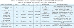
The table shows an example of analysis requirements that depend on SEE sensitivity. Heavy ion- and proton-induced SEE rates can be calculated in the presence of quiet and under solar event conditions.
GaN HEMT Displacement Damage Dose effects
Displacement damage dose (DDD) parameter degradation in GaN HEMTs will happen at DDD levels higher than those for typical space applications.
DDD effects in GaN HEMTs:
- A threshold voltage shift (typically positive)
- Decreased drain current
- Decreased mobility and transconductance
DDD susceptibility becomes greater when:
- Component parts are biased during irradiation
- Parts have had prior hot-carrier stress
GaN HEMT Total Ionizing Dose
GaN FETs in power applications open the door to new technology trends in the cold void of outer space. Demand is great for an easy-to-use pulse-width modulation (PWM) controller, with a high-reliability integrated circuit (IC), which will be able to directly drive GaN power FETs.
In previous research, COTS GaN power transistors were exposed to TID effects via 10-keV X-rays. Such GaN HEMTs were tested in both on- and off-state bias conditions. These GaN switching tests were conducted before, during, and after irradiation, and the devices were characterized at temperatures ranging from −50 to +75°C. The results indicate that GaN technology, with a bandgap of 3.4 eV, is a promising candidate for use in harsh environments.
HEMT devices have heterojunctions, in which electrons are confined to a quantum well, thereby avoiding impurity scattering. These devices are also known as two-dimensional electron gas field-effect transistors (TEGFETs).
Summary
GaN devices exhibit significantly higher radiation hardness than their Si and GaAs counterparts, primarily due to the high bond strength in III-nitride materials. GaN’s response to radiation damage is a function of radiation dose, type, and energy, coupled with carrier and dislocation density, as well as impurity content density.
Rad-hard by design makes possible applications requiring a very high-dose tolerance for ICs, while also meeting demanding electronic and reliability performance guidelines in the space and military industries.
>>Download the PDF of this article
About the Author
Steve Taranovich
Freelance Technical Writer, Phoenix Information Communication LLC
Steve is a contributing editor to Electronic Design.
Author of the non-fiction “Guardians of the Right Stuff,” a true story of the Apollo program as told by NASA and Grumman Corp. engineers, an astronaut, and technicians.
Experienced Editor-In-Chief of EETimes/Planet Analog and Senior Technical Editor at EDN running the Analog and Power Management Design Centers from 2012 to 2019.
A demonstrated history in electronic circuit design and applications for 40 years, and nine years of technical writing and editing in industry. Skilled in Analog Electronics, Space-related Electronics, Audio, RF & Communications, Power Management, Electrical Engineering, and Integrated Circuits (IC).
1972 to 1988 worked as a circuit design engineer in audio (8 years) and microwave (8 years). Then was Corporate Account Manager/applications engineer for Burr-Brown from 1988 to 2000 when TI purchased Burr-Brown. Worked for TI from 2000 to 2011.
Strong media and communication professional with a BEEE from NYU Engineering in 1972 and an MSEE from Polytechnic University in 1989. Senior Lifetime member of IEEE. Former IEEE Long Island, NY Director of Educational Activities. Eta Kappa Nu EE honor society member since 1970.
Comment About the Article
To join the conversation, and become an exclusive member of Electronic Design, create an account today!

Leaders relevant to this article: