Apply Tee Networks to Broaden TIA Required Solutions (Part 2): Loop Gain Plot, Noise, and Single-Supply Operation
What you'll learn:
- Modifying the loop gain plot with the tee network.
- Obtaining total output integrated noise with the tee network.
- How to modify the design to a single supply.
- Using a JFET input device to apply the tee network.
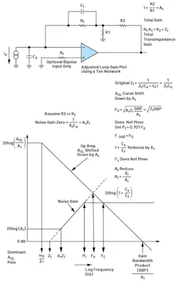
The tee network algebra of Part 1 can be illustrated by adjusting the terms in-the-loop gain (LG) plot. It gives a visual interpretation of what the tee network is doing.
This article discusses the effect the tee network has on the different output spots and then assesses the integrated noise terms. The required circuit modifications to operate the transimpedance amplifier (TIA) with the tee network using a single supply are shown. Testing the tee in adapting a very demanding 50-MΩ TIA design is then executed, raising the required feedback Cf to equal a typical 0.2-pF parasitic value.
Modifying the LG Plot with the Tee Network
One way to approach the compensation solution for this tee network idea is to adjust each part of the original LG plot of Figure 2 in Part 1, including the effect of that inside-the-loop tee network. The adjustments to get the plot of Figure 1 include:
- The low frequency noise gain shifts up to 20log(At).
- The Z1 frequency will move out in frequency by At as well.
- The inside of the loop tee divider has effectively shifted the amplifier’s Aol curve down by that amount. The entire Aol curve shifts down by 20log(At).
- Since Z1 has shifted up the same amount as the gain bandwidth product (GBP) has shifted down, the Fo frequency remains the same.
- Staying with the Butterworth target of setting P1 = 0.707 × Fo, that frequency hasn’t moved with the addition of the tee. Hence, using that lower Rf value, now that we have some tee gain, will shift the required Cf up — maybe into a realizable range for particularly challenging designs.
- The higher frequency noise gain (NG) set by 1+ Cs/Cf has moved down by the At gain, which, along with the amplifier Aol curve shifting down by At, places the Fc frequency at the same place as the design without the tee.
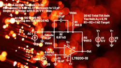
Applying these LG curve modifications to the example of Figure 5 in Part 1 using a tee gain of 2.78 adjusts the key elements on the LG curve to:
- Low-frequency noise gain goes up to 20log(2.78) = 8.9 dB.
- Z1 (1/2πRfCs) shifts out to 1.63 MHz (from a no tee 556 kHz, 2.78×).
- The effective GBP shifts down to 1.3 GHz/2.78 = 467 MHz.
- The geometric mean of Z1 and GBP (Fo) stays the same at √1.63 MHz × 467 MHz = 27.6 MHz.
- Set the feedback pole at the same 0.707 × Fo = 0.707 × 27.6 MHz = 19.5 MHz.
- The higher Cf value reduces the higher-frequency NG to 1 + 14.3 pF/1.2 pF = 13. That then intersects the lower GBP curve at the same Fc frequency, Fc = 467 MHz/13 = 35.9 MHz. The tee gain has also shifted the minimum stable gain down to 10/2.78 = 3.6, where the new NG2 = 13 comfortably exceeds that.
Total Output Integrated Noise Using the Tee Network
The gains for each of the noise terms will be changed when going to the tee network, except for the op amps’ input current noise, which, by definition, will have the same resistive gain using the tee. The input spot voltage noise gets to the output × the noise gain curve, then is band-limited either at the Fc frequency or by a lower bandwidth noise power bandwidth (NPBW) limiting postfilter.
The tee will increase from a gain of 1 to a gain of At from low frequencies to the new noise gain zero frequency that’s shifted up from the no tee location by the At gain. That will be an increased contribution using the tee, but this part of the output integrated noise is usually a very small part of the total and doesn’t increase the total by more than 0.5%.
>>Download the PDF of this article, and check out Part 1 of this two-part series
The rising portion of the NG curve will add an equivalent spot noise for integration through P1 that’s identical to the original no tee design. If the NPBW is higher than the P1 frequency (where the NG goes flat at the now reduced higher-frequency NG set by 1 + Cs/Cf), it’s then gained up by the tee gain to be at the same output level and has the same flat span from P1 to Fc.
The more significant part of the output integrated noise that’s automatically increased by the tee network is the Johnson noise for the feedback resistor. Analyzing that term’s spot noise with just the simple Rf resistor and then the solution using a tee network shows that it increases by a √At factor. Looking at the original spot noise voltage term, due to the Rf noise, will give:

Output spot noise due to the Rf Johnson noise (no tee) will give:
Neglecting the small R2 term in the gain and output noise, going to the tee network reduces Rf by At. However, it then multiplies that spot noise by a linear At value. That adjustment is shown here: Rf’ is the reduced Rf value by At neglecting the small effect R2 has on the TIA gain and output noise.
From a spot noise perspective at the op amp output, the contribution of the original Rf Johnson noise has been increased by √At. Often, the resistor noise part of the total equivalent integrated output Vo RMS is a small part of the total. If so, this adjustment will increase the total integrated noise only slightly. The Rf in these equations is the original desired gain.
In the example design (Figure 5, Part 1) with NPBW set to 20 MHz, the “no tee” design is dominated by the input current noise × the Rf gain as 86% of the total output noise power. With the tee design, targeting Cf = 1.2 pF increases the simulated integrated noise over 20 MHz from 330 µV RMS with no tee to 351 µV rms (only 6%). The Rf noise contribution increases from 6% of the total to 15% with that √At multiplier in its spot noise to the output.
Modifying the Design to a Single Supply
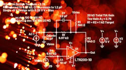
Most TIA designs operate from a unipolar output diode where the op amp is operating with a single supply, and the zero input output voltage is set just above the negative supply rail to keep the output stage out of saturation for a faster, more linear response. The easiest way to operate with an actual ground on the V+ input (part of the diode bias voltage) is to provide a small negative supply (such as –0.25 V) to give adequate headroom to the output stage for typical RROUT devices like the LT6200-10.
Lacking that negative supply, Figure 2 shows the design modified to a single 5-V supply with the inputs and output biased to approximately 0.25 V with no diode input current. With that offset on the V+ input, that same voltage will need to be applied to the bottom of the R1 resistor in the tee network to remove it as an output offset term.
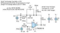
This nominal simulation shows 0.236 output DC bias. The VBIAS source into R1 must show a low broadband output impedance with low noise for good broadband TIA performance. Consider buffering VBIAS into R1 using the ADA4899-1.
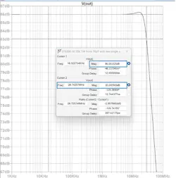
The small signal AC response of Figure 3 operating with a single +5-V supply has peaked at a very slight 0.25 dB and rolled off at 28.8 MHz — a very slight shift from the supply-centered response using split ±2.5-V supplies of Figure 6 in Part 1. This slight closed-loop response peaking over the balanced supply case is likely due to small shifts in the internal Aol curve. That 0.25-dB peaking maps to a closed-loop Q = 0.8, where a nominal 9% step overshoot should be expected.
Producing a 0.25- to 2.25-V output square wave at 2 MHz is shown in the waveform of Figure 4. This overshoots the expected 9% and reveals a good reason to have a little extra headroom on the negative side to keep any overshoot from clipping into the negative supply.
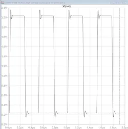
Adjusting the Cf up slightly can be used to reduce this overshoot. Any kind of post-NPBW filter can also be used to reduce this overshoot and should be considered in these designs to control the integrated noise.
Applying the Tee Network Using a JFET Input Device
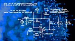
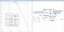
To illustrate how useful this tee network technique might be, implement a 50-MΩ design from a 100-pF detector using the unity-gain stable AD8065 JFET input FastFET device. The design equations shown here apply equally as well to this unity-gain stable, 67-MHz GBP, very low input bias-current device.
For very high TIA gains, JFET or CMOS inputs are preferred to remove the output DC offset due to the input bias current through that feedback resistor. The simple design required a 0.1-pF Cf, too low for implementation. Targeting a 0.2-pF parasitic in the Rf resistor requires the tee design of Figure 5, where the Rf element has been reduced from 50 MΩ to 25.4 MΩ, and relatively low-valued R1 and R2 elements provide 1.97 At gain. The expected F-3dB in a Butterworth response was verified in this test simulation at the expected 44 kHz.
Note that there’s no matching resistor on the V+ input to ground, as this JFET input device doesn’t have matching input bias currents. The maximum 6-pA input bias current (25°C) adds only 6 pA × 50 MΩ = 0.3 mV to the output offset error. The 25°C max input offset voltage of 1.5 mV now adds 1.97 × 1.5 mV = 2.96 mV output offset error.
Simulating the total output integrated noise through 30 kHz for the simple design shows 732 µV RMS (input-referred 14.7 pA RMS), where the tee design increases to 743 µV RMS. This is only a very slight increase since, in this design, the dominant noise term is the peaking NG × the 7-nV input voltage noise for the AD8065, which adds terms that don’t really change going to the tee design.
Conclusion
When a TIA design asks for a possibly unrealizable low Cf value in the simple TIA design flow, using a resistive tee network is one simple option to raise the required Cf. Furthermore, it provides the same gain and SSBW at the possible cost of a small increase in output integrated noise.
This simple approach can also be used more generally to move the required Cf exactly onto standard C values for easier implementation. Be sure to account for the typical 0.20-pF parasitic on resistors. The tee network will reduce the input common-mode voltage shift, too, due to a bias-current cancellation resistor on the V+ input used for bipolar input op-amp solutions. Be sure to add a noise band-limiting cap for the resistor into the V+ input if that bias-current balancing resistor is used.
>>Download the PDF of this article, and check out Part 1 of this two-part series
About the Author

Michael Steffes
Analog Signal Path Consultant
Starting as an IC design engineer at the original current feedback amplifier company (Comlinear), I progressed through 35 years of high speed amplifier development projects. Through these years I contributed to the definition, development, and product launch (datasheets and simulation models) of over 150 high speed amplifiers. Generating the related technical collateral also produced over 150 contributed articles and application notes..
Comment About the Article
To join the conversation, and become an exclusive member of Electronic Design, create an account today!

Leaders relevant to this article: