Apply Tee Networks to Broaden TIA Required Solutions (Part 1): Compensation Flow
What you'll learn:
- Four-step process for a compensation flow for an approximate closed-loop Butterworth response in a TIA design.
- Improving a TIA design by adding a resistive tee network.

Optical sensing requirements seem to be everywhere and growing fast. Extant literature approaches the design solutions from multiple directions. What’s presented here is a relatively simple, approximate design solution.
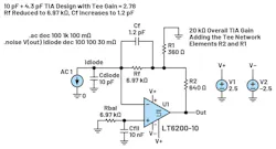
Figure 1 illustrates the basic photodiode transimpedance amplifier (TIA) design problem. The key elements are identified using the 1.3-GHz, gain-bandwidth-product (GBP) LT6200-10 decompensated voltage feedback amplifier (VFA).
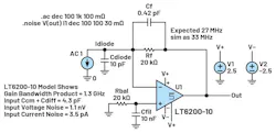
This is a specific example using a 10-pF detector diode (under its intended reverse bias voltage, not shown in Figure 1) targeting a closed-loop second-order Butterworth frequency response for a 20-kΩ desired gain from the input current to the output voltage. But first, a few important points.
Key Considerations
1. This bipolar input device has a relatively high input bias current coming out of the input pins when operated close to the negative supply. Rail-to-rail input stages (like the LT6200-10) have a crossover close to the positive supply where a different input stage is activated.
For TIA designs, the input pins are normally biased toward the negative rail and don’t move in a common-mode (CM) sense. There, the PNP input stage shows a typical 18-µA bias current coming out of the pins for the online SPICE model. The Rbal resistor will cancel the output DC error due to this bias current down to an Ioffset × Rf term, and Cfil is added to attenuate the Johnson noise from Rbal.
This nominal 18 µA input bias current through Rbal = 20 kΩ will shift the V+ node (and input pins) positive by 0.36 V, which will also add to the photodiode bias voltage. The specified maximum 4-µA input offset current will add 4 µA × 20 kΩ = ±80 mV to the output DC error band in this example.
2. This starting point is a balanced bipolar supply, so the initial tests are supply centered at ground. Normally, diode detectors are unipolar output current (shown sinking in Figure 1), and the circuit will bias the input and output to swing from some minimum voltage level unipolar positive. A single supply modification to Figure 1 will be considered later.
3. It’s important to add the parasitic input Ccm + Cdiff to the diode source capacitance for compensation analysis (setting Cf). Testing the LTC6200-10 LTspice model showed Ccm = 3.6 pF and Cdiff = 0.7 pF. Therefore, for the design, add 4.3 pF to the source (10 pF in this example) and use this total Cs = Cdiode+ Ccm+ Cdiff in the design equations. (The datasheet shows higher values, but for this work, the simulation model elements need to be used.)
4. The datasheet quotes 1.6-GHz GBP, but for TIA compensation, the noise gain will be crossing over the amplifier’s Aol curve at a relatively high noise gain. Hence, for TIA design, the single-pole projection to unity gain for the Aol curve is needed in the region where the Aol phase is approximately 90 degrees to estimate the correct GBP number of compensation solutions. That extracts to 1.3 GHz for the online simulation model.
5. The example design of Figure 1 shows a 0.42-pF feedback capacitor as Cf. A few simple steps will show how to derive this estimate using the loop gain (LG) curve of Figure 2. This is the typical LG curve for most TIA designs, where the amplifier’s open-loop gain curve has the feedback noise gain (NG) response superimposed on it to show the key frequencies in the design.
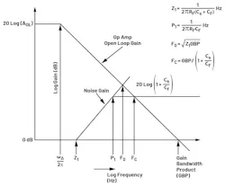
The key frequencies are shown on the LG graph in Figure 2.
Noise Gain
Fo will be the characteristic frequency of the second-order closed-loop Vout/Idiode frequency response. It’s the projection of the rising noise gain from a zero frequency (Z1) intersecting the device Aol response. Mathematically, it’s the geometric mean of Z1 and the GBP of the amplifier. A single-pole op-amp Aol model is usually adequate for this simplified design flow.
The noise gain will start rising at Z1 given by 1/(2π × Rf × (Cs+Cf)). A very useful approximation is to recognize that Cf is normally less than Cs, and perhaps Cf can be dropped from the Z1 expression for an approximate solution. Since that approximation on Z1 goes through a sqrt in the Fo expression, the error will usually be very small.
>>Download the PDF of this article, and check out Part 2 of this two-part series

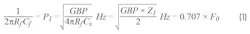
The compensation problem here is setting the noise gain pole: P1= 1/(2πRfCf), or simply Cf in this case if Rf is already chosen. A detailed analysis of the second-order Laplace transfer function for Figure 1 will reveal the closed-loop second-order response Q ≈ (P1/Fo). This very useful result gets even simpler if targeting Q = 0.707 (set P1 = 0.707 × Fo); the resulting closed-loop response will approximate a maximally flat Butterworth with F-3dB = Fo.
Four-Step Solution to Achieve TIA Closed-Loop Butterworth Response
This yields a simple four-step solution for Cf to give a TIA closed-loop Butterworth response. Using the example design above:
1. Find the approximate noise gain zero (1/(2π × 20 kΩ × 14.3 pF)) = 556 kHz. (This is neglecting the Cf that’s being solved for in the exact Z1 equation.)
2. Use this noise gain zero (Z1) and the amplifier’s GBP to estimate the Fo = √(556 kHz × 1.3 GHz) = 26.9 MHz = F-3dB for this Q = 0.707 design target.
3. Set the feedback pole at 0.707 × Fo, or 0.707 × 26.9 MHz = 19 MHz = P1. Or Cf = 1/(2π × 19 MHz × 20 kΩ) = 0.42 pF.
4. Check that the high-frequency noise gain is greater than the amplifier’s minimum stable gain, or 1 + (14.3 pF/0.42 pF) = 35 V/V is greater than the specified minimum stable gain of 10 V/V. This gives an Fc in the LG plot of Figure 2 at 1.3 GHz/35 = 37 MHz.
A Butterworth second-order target design will give a 65.5-degree phase margin (for an ideal single-pole Aol). This will be very stable if the higher-order Aol poles are far beyond the Fc frequency, which will be the case here. From this simplified Butterworth target design, any other desired Q may be delivered by simply scaling the feedback Cf value by that Q ratio.
Many legacy TIA design flows have targeted a Q = 1 by putting the feedback pole at Fo. To get that result, simply scale the Butterworth Cf down by 0.707/1 to produce that 1.2 dB peaking with 16% step overshoot result that comes with a Q = 1 second-order response.
Testing the small signal AC response for the LTspice circuit of Figure 1 gives the reasonably flat response of Figure 3. This isn’t a second-order shape as the Aol curve in the LT6200-10 model shows a higher-frequency zero/pole pair. However, at 33 MHz, F-3dB is reasonably close to the simplified design flow predicting 27-MHz F-3dB for this idealized Butterworth design.
Collapsing this design flow into a few simple equations will give this solution for P1, the feedback pole:
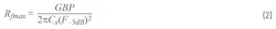
And then manipulating the equations for max Rf or max F-3dB given a device GBP and total source Cs leads to:
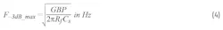
Or, solving this for max F-3dB, given some Rf and GBP, assuming the P1 is being set at 0.707 of:

And then solving this last equation for the minimum required GBP given a target F-3dB, Rf, and Cs will produce this constraint:

Clearly, for a given source capacitance, the GBP, Rf, and F-3dB are tightly coupled. For a given GBP and Cs, achieving more gain will reduce the bandwidth. Conversely, needing more bandwidth will require reducing the Rf value (gain).
How Adding a Resistive Tee Network to a TIA Design Helps
The example in Figure 1 asks for a relatively low 0.42-pF feedback capacitor. Typical surface-mount device (SMD) resistors used for Rf will have 0.18- to 0.2-pF parasitic, so the actual physical external Cf needs to be reduced to 0.22 pF.
While that might be achievable, using a small amount of in-circuit tee gain can shift that required Cf value up into a much more repeatable region. Or, when the required Cf is <0.20 pF, the gain can shift it up to that parasitic value with some amount of tee gain inside the loop.
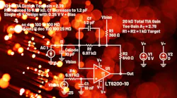
Figure 4 shows the starting point for a TIA design using a feedback tee inside the feedback loop.1
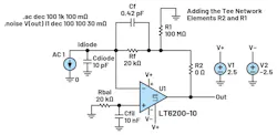
Leaving R1 out of the circuit for now, increasing R2 from 0 will add R2 to Rf in the TIA gain. For instance, setting R2 = 1 kΩ will increase the TIA gain to 21 kΩ in Figure 4. As the R1 element is also brought into play, that 1 + R2/R1 = At gain on the voltage at the output of Rf will increase the overall TIA gain from Rf + R2 up to Rf × At + R2.
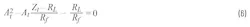
Looking first at the DC gain and offset effects of adding R1 and R2, and targeting a total TIA gain of Zt:
- Sweeping across different R1 and R2 solutions, typically using relatively low resistor values to keep their noise out of the total integrated output noise expression, try to hold the sum of R1 + R2 = Rl at some target op-amp load. Usually that will be the load used for the Aol curve generation.
- As the At gain is ramped up from 1 (no R1 in the circuit), the required Rf value will ramp down as Rf = Zt – R2/At.
- Given an Rl and Zt, solving for R2 and R1 as At is ramped up from 1 gives the following:
- R2 = Rl × (At – 1)/At
- R1 = Rl/At
- To retain input bias current error cancellation as Rf is being reduced (for a bipolar input op-amp solution), reduce Rbal to equal the new Rf value. This cancels the error voltage at the output of the Rf element due to matched input bias current terms in most bipolar input op amps. There will still be an input offset voltage error that will get an increasing gain to the output by the At gain. Where the input bias currents are relatively large (as in this bipolar input LT6200-10), reducing these Rbal = Rf values also reduces the input CM voltage shift due to Ib+ into Rbal. This can be very useful in higher targeted TIA gains (Zt) to keep the input CM voltage in range. JFET or CMOS input op-amp solutions would not use an Rbal element, as their input bias currents are much lower and not normally matched.
- For compensation, it will turn out that the feedback pole (P1) location set by a now reduced Rf value will stay constant, forcing the Cf value up. This can be very useful to increase Cf into a more realizable range.
Adding a tee network has increased the required Cf for any target design while also lowering the required Rbal value in bipolar input solutions, thus reducing the input CM voltage shift due to input bias currents. It’s also increased the gain for the op amp’s input offset voltage by that tee gain over the simple TIA design and slightly increased the output integrated noise.
Normally, this approach would use modest levels of tee gain to get the Cf value at or above parasitic levels. Simply selecting a desired tee gain would proceed as follows:
1. Choose an At value.
2. With a target R2 + R1 loading set as Rl, solve for R2 = Rl × (At – 1)/At.
3. Then R1 = Rl/At.
4. Reduce the Rf value to get the desired Zt gain using Rf = (Zt – R2)/At.
5. Use this new Rf value and the no tee P1 location to solve for an increased Cf = 1/2π × Rf × P1.
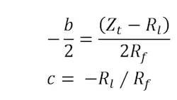
An alternate approach would be to target a specific Cf value, then proceed to set the other elements in the design. That approach will yield a quadratic solution for At:
Using the original no tee P1 location, targeting a particular Cf will solve for the required Rf value to get that same P1 location in the eventual tee network solution. Also constrain R1 + R2 = 1 kΩ = Rl. With a new Rf resolved, the quadratic solution for At needs these standard elements in the quadratic formula:
For the previous example design, target a feedback Cf of 1.2 pF. This will be 0.2 pF parasitic in the feedback resistor and a 1-pF external Cf. Holding the target P1 at 19 MHz requires Rf to go down to 6.97 kΩ.
From there, solving the quadratic will give At = 2.78, where R2 = 640 Ω and R1 = 360 Ω will deliver that Zt = 20 kΩ with Rl = 1 kΩ. Changing the example TIA design in LTspice to these conditions leads to the circuit of Figure 5.
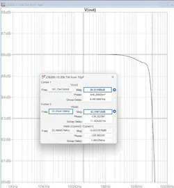
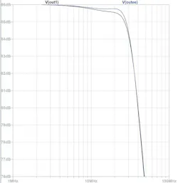
This new TIA response shape is overlaid on the original no tee design in Figure 6, showing almost no change in the simulated small signal frequency response. Both start out at 86-dBΩ gain (20 × log(20 kΩ)), with a bit of ripple and the Vout tee network riding a little higher, but both hit 33.7 MHz F-3dB.
It’s commonly thought that a tee network will significantly increase the integrated output noise. Such an assessment depends strongly on the anticipated noise integration bandwidth.
Briefly looking at the simulated output integrated noise through 20 MHz shows a very slight increase from 330 µV rms for the simple 20-kΩ feedback of the Figure 1 design, to 363 µV RMS for the tee network in Figure 5. By far the dominant contributor in both is the relatively high input current noise term of 3.5 pA/√Hz × the 20-kΩ gain to the output. The gain for input current noise doesn’t change when going to the tee network approach from the equivalent single resistor design.
It’s often useful to target a TIA bandwidth beyond the desired channel bandwidth and constrain the noise integration bandwidth to something lower with a postfilter.
Conclusion
A simplified design flow to apply a tee network to a TIA design has been shown to raise the required compensation capacitor above parasitic levels. Part 2 illustrates the tee network graphically in an LG Bode plot, then describes the output noise impact using the tee, and concludes with a very challenging 50-MΩ TIA example design.
Reference
1. Jerald Graeme. Photodiode Amplifiers: Op Amp Solutions. McGraw Hill, December 1995.
>>Download the PDF of this article, and check out Part 2 of this two part-series
About the Author

Michael Steffes
Analog Signal Path Consultant
Starting as an IC design engineer at the original current feedback amplifier company (Comlinear), I progressed through 35 years of high speed amplifier development projects. Through these years I contributed to the definition, development, and product launch (datasheets and simulation models) of over 150 high speed amplifiers. Generating the related technical collateral also produced over 150 contributed articles and application notes..
Comment About the Article
To join the conversation, and become an exclusive member of Electronic Design, create an account today!

Leaders relevant to this article: