Digitally Controlled Current Limiter Safely Charges Large Capacitor Banks
At a power-on cycle, inrush current, if not limited, can peak to tens of even hundreds of amps when capacitive load is present, thereby increasing the probability of failure and decreasing usable lifetime of a device. With large capacitor banks, an inrush current limiter is a necessary component.
A MOSFET as a voltage-controlled current device is perfectly suitable to be part of an inrush-current limiter. Power supplies with pulsed current across a current passing MOSFET at increasing duty-cycle rate are very common inrush-current limiter designs with active components. However, such designs stress the MOSFET due to currents often order of magnitude higher than the maximum safe current in a dc mode.
This current-limiter circuit design idea is based on a feedback-controlled current, where current across a MOSFET rises with an increase of the actual voltage across the capacitor bank Vcap (Fig. 1). Based on that voltage, a controller sets the maximum charging current while current limit is controlled through a real-time feedback sense of the charging current.
1. The maximum charging current is established by a controller that measures the voltage across the capacitor bank during charging cycle.
Charging current is determined based on a MOSFET safe-operating dc curve; its maximal drain current is a function of drain-to-source voltage (VDS). VDS is the difference between rectified ac input voltage, and Vcap in this design idea. Current rating also depends significantly on MOSFET temperature. For example, the datasheet for the APT75M50L N-channel MOSFET used in this design idea shows that in dc mode, the maximal current is ≈1 A at VDS = 300 V, and ≈4 A at VDS = 100 V at a case temperature of 25°C and junction temperature of 150°C.
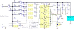
In the practical circuit design (Fig. 2), U1 through U5 are photovoltaic MOSFET drivers. For the circuit to operate, U1’s driver is first activated via the digital on/off control pin, which in turn drives power MOSFET Q1 (the control element). With U1 active and the capacitor bank at 0 V, the charging current is set by R3, while Q2 acts as current limiter controlling the gate-source voltage of Q1. At this stage, Q3 through Q6 are not conducting and given Q2’s VBE = 0.48 V, the charging current is set and limited to 0.48 V/R3 ≈ 0.5 A. Resistors R16 through R23 form voltage dividers, providing a measure of the capacitor bank voltage for the quad comparator U6 (LM339), which uses a reference voltage of 2.5 V from the bandgap reference U7.
2. Photovoltaic gate drivers control the MOSFETs, which, in turn, control and step the current flow.
The role of each comparator is to control conductivity of branches with resistors R4 through R7 being either conductive or cut off, therefore setting different current limits depending on the Vcap. With the given resistor values, comparators U6A to U6D will be triggered when the Vcap exceeds approximately 60 V, 120 V, 175 V and 215 V, and will make branches with R4 through R7 respectively conductive.
For example, when the Vcap exceeds 60 V, it will trigger comparator U6A, setting its output low. This turns on MOSFET driver U2, driving Q3 into a fully conductive mode, and the branch with R4 will start to conduct current in parallel with R3. The charging current passing through Q1 is now determined by a parallel combination of resistors R3 and R4 + RDS (the on-resistance of Q3, maximum value 40 mΩ), while Q2 maintains the same current-limiting function. The new current limit is 0.48 V/(R3 || (R4 + RDS) ≈ 0.9 A.
A printed-circuit board was built and tested extensively to prove the robustness and efficiency of this circuit. The input voltage is rectified 240 V ac from a 120/240-V ac transformer. The charging current was measured across a 1-Ω resistor with an isolated oscilloscope probe. The approximate maximum current levels were 0.5 A for Vcap of 0 to 60 V; 0.9 A for Vcap of 60 to 120 V; 1.5 A for Vcap of 120 to 180 V; 2.25 A for Vcap of 180 to 215 V; and 5.7 A for Vcap above 215 V.
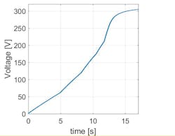
3. The voltage versus time graph shows inflection points (knees) where the charging current changes.
In the graph of the Vcap during its charging cycle (Fig. 3), the different knee points illustrate different charging currents, quantified with a changing slope of the line. Resistors R1 and R8 through R11 are fail-safe measures that keep the MOSFETs shut off in a case of open-circuit failure of photovoltaic MOSFET drivers. VCC can be either 3.3 V or 5 V with the given resistor values, or higher if resistor values R2, R12 to R15, and R24 are appropriately re-scaled.
Ilija Uzelac is a Research Scientist at Georgia Institute of Technology, with a PhD in Physics from Vanderbilt University, and a Master’s in Electrical Engineering from University of Belgrade, Serbia.
References
1) Ilija Uzelac, "Feedback-Controlled Constant-Current Limiter Includes Digital On/Off Control," Electronic Design.
2) Ilija Uzelac and Ron Reiserer, “Series-connected MOSFETs increase voltage & power handling,” EDN.
About the Author
Ilija Uzelac
Research Scientist
Ilija Uzelac is a Research Scientist at Georgia Institute of Technology, with a PhD in Physics from Vanderbilt University, and a Master’s in Electrical Engineering from University of Belgrade, Serbia.
Voice Your Opinion!
To join the conversation, and become an exclusive member of Electronic Design, create an account today!

Leaders relevant to this article:


