Integration has long been the key to the adoption and growth of microelectromechanical-systems (MEMS) technology. MEMS-based devices are already used in a broad range of electronic products, from audio microphones for sound to optical components for displays and vision, and should only continue to expand into different application areas.
With a growing number of commercial MEMS foundries, opportunities are increasing to experiment with MEMS design approaches. Future success may depend on how well they can combine MEMS technology with their current blend of semiconductor and other electronic technologies.
This file type includes high resolution graphics and schematics when applicable.
Popular Applications and Devices
MEMS devices are chips that combine electronic and mechanical functions. They can be mass produced using modified semiconductor processes using substrate materials such as silicon to form mechanical parts, like switches and sensors, on the same chip as transistors and ICs. Three-dimensional (3D) structures are typically formed on the substrates for the mechanical portions of the device, which may include levers, hinges, and gears, with actuators controlling mechanical motion.
Actuators may control motion by means of electrostatic, magnetic, or thermal energy. A human body can even be the source of energy for a MEMS device. The MEMS structures can be used for small machines that produce different motions or for sensors that detect and measure small motions, such as acceleration in car engines and blood pressure in medical applications.
The largest market for MEMS technology right now is at audio frequencies for microphones in smart phones and other portable communications devices. MEMS-based sensors are already well established and widely used in many consumer electronics applications, including gaming consoles, computer tablets, and navigation devices. MEMS pressure sensors are also used extensively throughout modern automobile designs for measuring different fluids and gases, such as air-conditioner systems (see “MEMS Technology Gears Up For Big Innovations”).
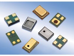
Improvements among the largest MEMS applications such as microphones areas are taking place on a regular basis. According to Knowles Corp., its SPH0641LM4H-1 digital MEMS microphone consumes a third the power of other digital MEMS microphones and boasts high signal-to-noise-ratio (SNR) performance in low-power mode (Fig. 1). It provides a low-power alternative to the use of an analog microphone and analog-to-digital converter (ADC).
Since it’s as much as 20% smaller than other models, the SPH0641LM4H-1 also does away with the previous tradeoff between designing a portable product and having to choose between a microphone with high SNR or one with low current draw. It handles 20 Hz to 20 kHz and measures 3.50 by 2.65 by 0.98 mm.
Similarly, the Knowles SPH0641LU4H-1 MEMS microwave provides ultrasonic bandwidth to 80 kHz for use in advanced applications with ultrasonic sound waves, such as touchless gesture recognition and phone-to-phone data transmission between smart phones.
The InvenSense ICS-40720 low-noise omnidirectional MEMS microphone consists of a MEMS microphone element, impedance converter, and output amplifier housed in a compact 4- by 3- by 1.2-mm surface-mount package. It provides linear response at sound pressure levels (SPLs) to 122 dB and offers sensitivity of –32 dBV, performance levels that compare favorably with more conventional, more expensive, and much larger discrete-element microphones.
MEMS sensors are also being used in large numbers, largely in automobiles for vehicular safety applications. More and more companies are already manufacturing many different types of MEMS-based sensors. Some of the leading developers are investing in improved fabrication capabilities for possibly integrating MEMS technology with semiconductor and other microscale electronic technologies.
STMicroelectronics is establishing a pilot fabrication facility to process 200-mm wafers using a combination of MEMS, magnetic, and piezoelectric technologies on the same IC. The firm is one of the leading suppliers of MEMS sensors but is well aware of the growth potential for MEMS technology in many different application areas, with plans to eventually move that facility to 300-mm wafers.
Freescale Semiconductors has melded multiple technologies such as silicon MEMS and CMOS circuits as part of its Xtrinsic sensor products. These devices rely on a modular approach to combine multiple sensor inputs, logic, and other circuits into compact solutions. They are supported by customizable software to create sensor solutions that efficiently and effectively fill a customer’s requirements.
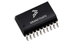
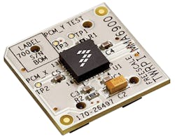
Freescale, which has been making MEMS sensors for almost 30 years, applies its high-aspect-ratio MEMS (HARMEMS) technology to many different automotive safety systems, including vehicular air-bag systems (Fig. 2). The same technology is being investigated for health-care monitoring applications, with MEMS pressure sensors used for patient diagnostic functions. The HARMEMS technology has also been used in dual-axis accelerometers for vehicular electronic-stability-control (ESC) systems to measure lateral acceleration. The firm also assists with development platforms that help customers integrate different MEMS sensors into their applications (Fig. 3).
The increasing number of sensors in portable electronic devices, vehicles, and even clothing is creating a growing need for what is known as “sensor fusion,” or the practical combination of data from the many different sensors (both MEMS and non-MEMS sensors) within a device or product. Within many portable electronic products, such as cellular telephones, sensor hubs are used to collect and analyze the results from different sensors for effective application.
Of course, sensor fusion can occur at different levels within a product, such as within an individual MEMS sensor, within a sensor hub, or within a microprocessor and software of a product, so some amount of data partitioning may be required as part of sensor fusion. The evolution of sensor fusion will enable applications that might not have been available previously, such as indoor navigation within a shopping mall, using a cellular telephone.
MEMS Components
MEMS devices are also moving into application areas where they can replace traditional technologies, such as semiconductor-based switches and oscillators, with lower-power alternatives. Some companies have developed MEMS-based clock oscillators as replacements for traditional quartz-crystal clock oscillators.
The DSC1102 and DSC1122 low-voltage-positive, emitter-coupled-logic (LVPECL) oscillators from Discera are based on silicon MEMS technology. They are available with frequencies from 2.3 to 460.0 MHz with low root-mean-square (RMS) phase jitter of typically less than 1 ps. The oscillators differ in their disable approaches, with the DSC1102 fully powering down in standby mode and the DSC1122 disabling its outputs in standby mode.
Both oscillators are qualified to MIL-STD-883 for shock and vibration and are available for the commercial temperature range of –20°C to 70°C or industrial temperature range of –40°C to 85°C. They can be supplied in very small footprints (2.5 by 2.0 mm, 3.2 by 2.5 mm, 5.0 by 3.2 mm, and 7.0 by 5.0 mm) with stability levels of ±10, ±25, and ±50 ppm as drop-in replacements for standard six-pin low-voltage positive emitter coupled logic (LVPECL) quartz-crystal oscillators. These lead-free and RoHS-compliant (Restrictions on Hazardous Substances) MEMS oscillators are designed for supply voltages of +2.25 to +3.60 V dc as well.
MEMS clock oscillators are available from a number of additional suppliers. For example, SiTime manufactures its oscillators with standard silicon CMOS semiconductor equipment. Based on a common resonator, they perform on-chip electronic tuning to achieve different output frequencies.
Silicon Labs’ Si50X CMEMS general-purpose oscillators are based on a combination of silicon CMOS and MEMS technologies. They feature a guaranteed 10-year operating lifetime at output frequencies to 100 MHz. They are available in single-, dual-, and quad-frequency models, with stability levels of ±20, ±30, or ±50 ppm and only 1.1-ps RMS jitter. The packaged CMEMS oscillators measure only 2.0 by 2.5, 2.5 by 3.2, and 3.2 by 5.0 mm.
Integrated Device Technology, a longtime supplier of traditional quartz-crystal clock oscillators, also has developed lines of MEMS clock oscillators based on its own silicon MEMS resonators. The MEMS oscillators provide LVPECL outputs at frequencies to 625 MHz with better than 1-ps phase jitter.
Although MEMS sensors have become large-volume components by merit of their use in cellular telephones such as 3G and 4G handsets, MEMS switches have also seen their fair share of use in these same applications. Omron Corp., perhaps most associated with its MEMS sensors and wafer foundry services, has offered its 2SMES-01 MEMS switch for several years. It is designed in a single-pole, double-throw (SPDT) switch configuration and rated for more than 100 million switching operations.
Measuring just 5.2 by 3.0 by 1.8 mm and operating with low current consumption, the 2SMES-01 boasts low insertion loss of just 1 dB at 10 GHz and high isolation of 30 dB at 10 GHz. The switch has a three-layer structure, on glass, silicon, and glass. The top glass layer provides a hermetic seal. The middle silicon section contains the actuator and movable electrode. The bottom glass layer is the base.
In addition to its MEMS oscillators, Radant MEMS has developed and has demonstrated MEMS switches capable of more than 1.5 trillion switching cycles in response to any concerns that the mechanical contacts in MEMS switches can degrade over time and with millions of switching cycles. The company recently introduced a pair of impressive MEMS-based switches for broadband, microwave applications.
The RMSW100HP single-pole, single-throw (SPST) reflective switch is supplied in hermetic die form for die-attach to printed-circuit boards (PCBs). It is designed for applications from dc to 12 GHz, with less than 0.17-dB insertion loss at 2 GHz and less than 0.28-dB insertion loss at 10 GHz. It exhibits switching speed of less than 10 µs and provides isolation of better than 23 dB at 2 GHz and more than 11 dB at 10 GHz.
For even higher frequencies, the RMSW200HP SPST MEMS switch features a frequency range of dc to 40 GHz and is also supplied in hermetic die form. It boasts 20-dB typical isolation at 10 GHz with better than 12-dB isolation at 38 GHz. It offers less than 0.4-dB insertion loss at 10 GHz and less than 0.5-dB insertion loss at 38 GHz. Both switches are rated for more than 10 billion switching cycles at normal RF/microwave power levels.
MEMS for Medicine
Many companies involved in MEMS development recognize how the technology can serve some critical applications in the health-care industry. With its combination of MEMS and many other microelectronic technologies, STMicroelectronics is applying MEMS designs to sensors and graphical display monitors for health-care products.
Different types of MEMS sensors are used in low-power portable devices for such functions as glucose meters and blood-pressure monitors, while MEMS motion, pressure, and magnetic sensors are applied to medical imaging applications. MEMS devices are often included with many other microsystem technologies for medical applications as “BioMEMS” devices.
Recently acquired by global medical device supplier St. Jude Medical, CardioMEMS has developed the CardioMEMSHF System, an implantable, FDA-approved (Food and Drug Administration), MEMS-based sensor. It is implanted in a patient’s pulmonary artery and monitors the heart for dangerous pressure buildup following cardiac surgery (Fig. 4). The system wirelessly communicates information from the sensor to the physician, allowing patient heart monitoring without hospitalization.
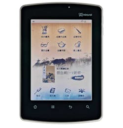
More than a few companies see MEMS technology as a viable approach for reflective-type miniature displays. Qualcomm, for example, has based its mirasol graphic displays on MEMS technology (Fig. 5). Based on the firm’s interferometric modulation (IMOD) technology to achieve low-power displays with high contrast ratios, mirasol displays are fabricated by means of MEMS and thin-film optics technologies. The first commercial displays will be bichrome, with two colors.
The IMOD consumes much less power than other display technologies, such as LCDs or organic LEDs (OLEDs), according to Qualcomm. It also offers much faster response times than competitive LCD technologies, which will reduce blurring when viewing fast-moving images, such as in video games. Not requiring a backlight, mirasol displays can be made much thinner than competing technologies. Time will tell if this use of MEMS technology will gain the popularity of microphones and pressure sensors in many portable electronic products.
Sizing Up MEMS Foundries
As MEMS technology becomes more widespread, more electronic manufacturers are exploring its integration in their own products. Working with one of the growing number of MEMS commercial foundries can make this process easier. MEMS foundries not only bring the necessary equipment and processing environments for designing and making MEMS products, they also offer the expertise and a willingness to share that knowledge with their customers.
To make it easier for customers to adopt MEMS technology, Micralyne has formed a partnership with CMC Microsystems to help reduce the costs and risks for MEMS developers. The partnership lets designers purchase part of a silicon MEMS fabrication run via a multiple-product wafer strategy, with CMC Microsystems spearheading the production run, rather than commit to the entire production run.
MEMS runs are based on Micralyne’s MicroGEM-Si process technology, well suited for fabricating MEMS devices such as inertial sensors and optical switches. For those not willing to share their production runs, customers can purchase a full fabrication run for working directly with Microlyne on its MEMS product design and fabrication.
Designers interested in obtaining MEMS foundry services have a growing list of choices, including Silex Microsystems. The MEMS foundry has supported the commercialization of a wide range of MEMS devices, including accelerometers, infrared (IR) sensors, mirrors, humidity sensors, and RF switches. It operates two independent high-volume fabrication facilities with 6- and 8-in. wafer capacities, respectively.
All of the Silex technologies leverage the company’s SmartBlock approach to applying modular methods for achieving the fastest possible way to stable production for a design without compromising performance and/or reliability. The end result is that foundry customers working with the Silex foundry can expect to bring their MEMS products to market in the fastest time possible.
Midwest Microdevices is benefitting from economic and educational support from such sources as the state of Ohio and the University of Toledo. This well-equipped MEMS fabrication facility employs LPCVD and plasma-enhanced chemical vapor disposition (PECVD) processes to deposit dielectric thin films with great precision and uniformity and a wide range of sputtering and evaporation capabilities to deposit metals, ranging from aluminum to gold, on those dielectric materials in forming many different MEMS structures and circuits (Fig. 6).
The foundry employs fully automated LPCVD batch furnace tubes to process as many as 50 wafers at a time with wafer-to-wafer uniformity of better than ±3%. Each furnace tube runs on its own microprocessor and under software control to precisely match a customer’s requirements while enabling support of smaller, specialized MEMS fabrication runs, including for optical MEMS devices. The foundry employs reactive ion etching (RIE), wet etching, and plasma etching for the precise control of MEMS features. Back-end processes include wafer dicing, laser dicing, laser drilling, and wafer probing.
The X-FAB MEMS Foundry offers impressive expertise in MEMS design and manufacturing capabilities, along with a wide range of analog and mixed-signal IC foundry capabilities in silicon-on-insulator (SOI), silicon CMOS, and BiCMOS device technologies and the knowledge and experience of how to merge these different microminiature circuit technologies within the same chip or package.
For designers seeking optical MEMS devices, Coventor backs its extensive foundry facilities and experience with electromechanical finite-element models developed with popular computer-aided-engineering (CAE) software design tools, including software from Cadence Design Systems and Matlab software from the Mathworks. By combining Coventor’s software simulations with its foundry tools, customers can achieve faster design turnaround times with results that are usually quite close to performance expectations.
Of course, the list of available commercial MEMS foundries is long and growing. Some offer precision e-beam-lithography services (and manufacturing to spot sizes as fine as 2.5 nm) and fast fabrication turnaround times.
MNX, which is a MEMS foundry as well as a form of technology exchange for many customers, offers excellent prototypying services for designers seeking to develop MEMS products in small- and medium-volume product runs before committing to large-volume production. It maintains contractual relationships with many of the leading higher-volume MEMS foundries for those customers wishing to make the transition from smaller- to higher-volume production runs.
About the Author
Jack Browne
Contributing Editor
Jack Browne, Technical Contributor, has worked in technical publishing for over 30 years. He managed the content and production of three technical journals while at the American Institute of Physics, including Medical Physics and the Journal of Vacuum Science & Technology. He has been a Publisher and Editor for Penton Media, started the firm’s Wireless Symposium & Exhibition trade show in 1993, and currently serves as Technical Contributor for that company's Microwaves & RF magazine. Browne, who holds a BS in Mathematics from City College of New York and BA degrees in English and Philosophy from Fordham University, is a member of the IEEE.


