Wearable Technologies Present Packaging Challenges
If you work in the electronics industry, you’ve heard the buzz about wearable technology. But the concept is not new, as wearable electronics have been improving the quality of our lives for nearly half a century. Truly portable electronics were enabled with the invention of the microprocessor back in the early 1970s. Since that time, the industry has been mass producing and miniaturizing digital wristwatches, hearing aids, portable music players, and more.
Related Articles
- It Takes A WaRPed Mind To Design Wearable Tech
- Gallery: Wearable Tech At CES 2014
- Watches Return As Wireless Wearables Materialize
While portable electronics are not new, the classification is rapidly changing. Advances in microelectromechanical systems (MEMS) now allow nearly seamless integration of an array of sensors to collect information. Microcontrollers have shrunk to the point that they can be hidden away neatly and consume very little power. Wireless communication and low power standards allow for a network of independently operating components to easily integrate with each other. Low-power LEDs and flexible display technology are close to bringing science fiction into reality. Today, many wearable concepts are only limited by power management and battery life, but that is also quickly changing as advances are being made in energy harvesting and wireless charging technology.
This file type includes high resolution graphics and schematics when applicable.
Portable Platforms
With nearly everyone carrying a portable computer to serve as a launching point to social media and social networks, the wearable market has a largely untapped potential. Many concepts of how to integrate electronics are still new and very much in the prototyping phase. Combining electronics and sensors to collect information is only one part of the wearable electronics industry. Innovative application development utilizing microcontrollers is the other, less obvious part. Yet as products and new concepts emerge, semiconductor packaging is paving the way for the integration of very diverse technologies. The wearables industry is poised to explode and innovations in electronic packaging are a major reason why.
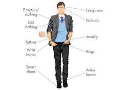
A large array of wearable products created quite the buzz at the 2014 International CES (Fig. 1). Gaining popularity with consumers are products like fitness and health trackers, smart watches and bands, sensing and touch-based e-textiles, personalized lighted clothing, and virtual reality displays, all creating unique challenges for packaging technology.
Fitness bands, which are essentially data collectors, can be found everywhere. They use accelerometers combined with contact and temperature sensors to track and log activity. Some integrate motor controllers with vibration for alerts, LEDs for status or light detection, and complex displays for more advanced interaction. Form factors must be small, flexible, and able to survive every environment that people live in.
Smart watches have similar expectations but add complex interactions between the touch display, cameras, and fast data communication with mobile platforms. Similar to the gadgets in early James Bond films, these devices eventually may replace or augment our use of mobile phones. As such, smart watches add even more complexity to wearables with high power and thermal management needs.
Further pushing the limits is the proliferation of portable heads-up displays (HUDs). Popularized by Google Glass, HUDs fully integrate all the elements of a smartphone into a convenient eyeglass-based platform. HUDs require cutting-edge miniaturization, interconnects, and thermal management.
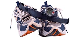
Other product ideas like smart e-textiles take a different approach. These textiles integrate stretch, pressure, and contact-based sensor elements that can be integrated within the fabric itself. Personalized clothing with LEDs and touch-based interaction has to be flexible with electronics and connections hidden away within the material. Even less conspicuous components are miniaturized and embedded in jewelry. Some applications integrated with clothing find very specialized roles, like the increasingly popular smart shoes for personal training. Electronics used in smart shoes are integrated with sensors in the sole to report weight distribution, stance, and movement.
All of these wearable electronics have similar functional requirements:
• The design and form factor of the electronics must be unobtrusive and nearly invisible.
• The electronic components have to be reliable enough to withstand the human environment and last the life of a product.
• Electronics in contact with skin must have a comfortable thermal operating range
Packaging plays a critical role in all of these areas.
Design And Form Factor
Form factor plays a major role in wearable technology—not just for the processor, but also the entire system. Chip-scale and wafer-based packaging are naturally finding a home in wearables with early adopters. Package size and integration of common functions are also important to wearables.
For demanding processor applications, the use of multi-chip modules (MCMs) with 2.5D and 3D integration achieves a small, thin form factor for applications like smart watches and Google Glass-type wearables. Minimizing wiring requirements outside of the package allows for easy integration onto miniature printed-circuit boards (PCBs).
Packages like quad flat no-lead (QFN), micro-chip-scale packaging (uCSP), and wafer-scale chip-scale packaging (CSP) are popular solutions for power management, microcontrollers, and wireless functions due to their small form factors. They can be used on small PCBs or integrated with use of flex-based circuits.
As more wearable applications are released and ramp to production, there will continue to be a shift to use system-in-package (SiP) to integrate the more common functions. Functions such as power management, sensors, and microcontrollers can be combined based on application use. Since many of the technologies involved require vastly different manufacturing processes, package integration is a natural next step to miniaturization and can offer some clear advantages to the system:
• Power footprint can be lowered as I/Os are optimized for near-field communication.
• Reduction in external I/O minimizes wiring in systems and allows faster communication between components.
• Exposure of components to the environment is reduced.
• Materials and process steps can be reduced, improving variation on end assembly and cost.
Reducing the form factor can include passives as well. While communication technology like Bluetooth has high-power demands and may work for some wearable products, most wearable technologies require lower-power transmission standards. These use radio transmission and radio-frequency identification (RFID). Integration of antennas on flex circuits, combined with wafer-scale chip on flex and SiP on flex, allow for a large array of possible form factors and solutions to be developed.
Thermal Considerations
Wearable electronics introduce some unique thermal design challenges for both the package and overall system. Operating temperature is not set by reliability requirements alone. The device also has to maintain a certain comfort level.
Electronics placed in direct contact with the skin need to maintain an ideal operating temperature at or below the core body temperature of 37°C (98.6°F). Anything above this is generally considered to be uncomfortable and hot (Fig. 2). Transitioning to much higher heat (above 40°C or 104°F) will trigger discomfort and pain for the wearer. This design challenge can be an issue for processor-intensive applications and units with complex displays.
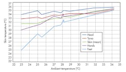
The good news for wearables is that the human body is also a great thermal regulator. Skin temperature is held below normal body temperature and can act as a sink to dissipate thermal energy (Fig. 3). This increases potential power consumption for wearables, depending on how and where the device will be worn, of course.
There are limits on what the body can regulate based on conduction and blood flow, but generally skin conductivity is ~0.37 W/mC. Thermal design is a challenge for products like smart watches and glasses that have high thermal demands on the processor and package. These products use packages and system solutions that optimize pathways to take advantage of skin contact. However, designers should still remain cautious when depending on the human body. Skin contact could be intermittent, affected by activity, or impeded by clothing. Also, if the device is removed, it is still expected to operate within the comfort zone.
Active thermal monitoring and power management is important to throttle back performance and prevent the device from exceeding the comfort zone. This requires adding thermal sensors on the silicon and in the system to monitor operation and power. The information is used in combination with clock management to make real-time adjustments in operation frequency. Ideally this function would integrate onto the processor, but it also can be combined using flex circuits or in the package to provide active monitoring.
Materials And Environment
The human body is not an ideal environment for electrical components. While the temperature range for worn devices may be limited, the environment itself can be harsh. Electronics are expected to function in very moist and dusty conditions. Fitness band manufacturers learned early on to design for everything from jostling and exposure to sweat in the gym to direct exposure to moisture in the shower. Many materials used in package and board assembly remain sensitive to moisture, requiring full encapsulation of all electronic components. Design has to address concerns for material interaction, reliability of interfaces, and impact on the thermal environment.
Concerns for exposure to certain elements and materials are also important to address. Packages need to not just be green, but also reflect the impact of skin-based sensitivities and standards defined for medical electronics. Meeting lead-free standards increasingly drives use of conformal coatings to reduce sensitivity for tin whisker growth. When a device is operating under strain, something more common in flex circuits, tin whisker growth can be accelerated. Use of conformal coatings on electronics as well as system-level encapsulation increases the number of material interfaces that can delaminate and fail if not properly designed.
Material interaction has both a chemical and a mechanical element driving calibration and testing to optimize the package, the coating, and even the encapsulation used in the end system. Less knowledgeable end customers typically will rely on the component manufacturer to ensure compatibility and to provide calibrated models for both mechanical assessment and reliability. Many of the mechanical-based interactions can be brought out with temperature-based cycling including moisture-based and pressure-based testing. Due to metal migration concerns, biased testing is increasingly important to validate sensitivity in moist environments and to validate the risk of tin whiskers.
Many companies have added requirements for package component bend testing, a direct result of the dominance of thin PCB, thin package, and flex-based circuits in wearables. The impacts of stretch and deformation extend further than the package connection to the PCB. Stress also can affect circuit operation, especially noticeable with MEMS used in sensors.
MEMS sensors rely heavily on components that detect changes in resistance or capacitance for metal and dielectric structures. When these structures deform, the values will change, causing a false signal or throwing off the calibration. Transistors on semiconductor wafers also can be sensitive to these effects as well. Stress causes deformation that changes how the transistor performs. As packages and system interconnects are made thinner, flex-based deformation is a real concern for electrical operation and reliability.
Without a doubt, circuit co-design extends to the package to ensure operation of the device under stress conditions. Analysis of stress on the semiconductor circuitry is highly complex and requires characterization of the package and silicon during development. In some ways the effects can be simplified by limiting the thickness and rigidity of the package and silicon interface.
To truly achieve the form factor requirements of wearables, a more complex circuit model and design is optimal to account for electrical variation and ensure performance. In this way, wearables will continue to blur the lines between circuit, package, and end system.
This just scratches the surface of packaging requirements for wearable electronics. Some products that are meant to integrate with clothing also have to address survivability while being cleaned or washed. Others require new models to represent shock and common wear and tear. Defining what is needed in terms of robust reliability testing for electrical components going into wearable products is certainly a new field in the making.
For now, the industry is still in learning mode as prototype and experimental products lead the way to more robust consumer offerings. From products with high expectations on lifetime to low-cost disposable devices, there is a wide expectation of how this industry will develop. There is clear evidence that as more and more applications find ways to use and process data from our everyday lives, wearables will continue to rely on innovations in packaging.

About the Author
Daryl Heussner
Senior Member, Technical Staff
Daryl Heussner is a senior member of the Technical Staff at Texas Instruments with over 18 years of experience in semiconductors and semiconductor packaging. He holds a BS in electrical engineering from Texas A&M University and has held roles supporting SI node process development, wire bond and flip packaging co-design, and package process development and roadmap. He was elected to the TI Technical Staff in 2000 for contributions in package design and later senior member in 2006 for contributions in the area of flip-chip BGA packaging. He leads a team at TI focusing on optimizing die and package co-design for manufacturing across TI package technologies.
Comment About the Article
To join the conversation, and become an exclusive member of Electronic Design, create an account today!

Leaders relevant to this article: