What’s Making Touchscreens Become So Thin…and Smart?
This file type includes high resolution graphics and schematics when applicable.
Capacitive touchscreen technology has revolutionized smartphones and tablets, and is finding its way into laptops, desktop PCs, and most recently automobiles and wearables. Due to the fiercely competitive market for these devices, vendors are constantly challenged to design systems with high display quality, ease of navigation, high performance, compact form factors, long battery life, and low cost. Because the touchscreen plays such an influential role in the user experience, the choice of its design can be a determining factor in a product’s ultimate success.
The ability to turn a display into a “touch screen” requires the seamless combination of two previously distinct functions—touch and display. Historically, adding touch sensors to the display has been handled autonomously by different companies supplying different layers in a laminated panel “stack-up” that’s assembled by a separate manufacturer. Recent technology advances have made it possible to integrate the touch sensors directly into the display, as well as integrate the touch controller and display driver functions into a single IC.
Advanced Touch Features
Touch sensors and controllers are being enhanced to deliver advanced user features such as:
- Touch wake-up gestures
- Pen support down to a 1 mm tip
- Concurrent finger and pen operation
- Proximity and finger hover
- Glove and fingernail support
- Ability to operate in moist environments
This article outlines the touch and display integration technologies currently available, including a new, fully integrated approach that could very well dominate future device designs. Before that, though, it describes the various ways touch sensors can be integrated directly into the display, followed by methods for integrating the touch controller and display driver functions into a single IC. The article also highlights the many advantages of integrating touch and display functions for both device manufacturers and their partners.
It’s important to note that this article focuses on smartphones and tablets with touchscreens smaller than 8 in. (20 cm). While it’s possible to integrate such touch and display functions in larger touchscreens using the methods described here, the differences are significant enough to warrant a separate overview.
Integrating Touch Sensors into the Display Stack-Up
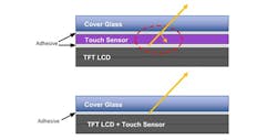
Generally, integrating the touch-sensing and display-update functions in a touchscreen device occurs in two areas: the display panel stack-up and the ICs controlling both functions. Figure 1 shows the many layers in the display and panel stack-ups in a typical touchscreen. Historically, touch sensors have often been added as a separate or discrete overlay atop the display in a laminated panel stack-up. With this design, the touch sensors are added either on the cover glass (CG) or in a dedicated sensor layer, typically made of plastic.
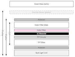
Putting the sensors on the cover glass lens is sometimes referred to as sensor-on-lens (SoL) or as a one glass solution (OGS), because it eliminates the need for a separate sensor layer. Designs with a separate sensor layer are known as glass-film (GF) or glass-film-film (GFF), depending on whether the transmitting and receiving touch functions are implemented in one or two layers, respectively, of the sensor film. All of these designs are called “discrete” to emphasize the fact that the touch function exists separately as an overlay on the display.
The discrete touch sensor overlay has the advantage of being a proven, low-risk design with a short time-to-market. Discrete designs are even used when implementing the latest display and touch technologies, which often get integrated in subsequent designs. Some LCD manufacturers (LCMs) also value the ability to leverage existing manufacturing setups in the plant and equipment. The disadvantage of discrete designs, though, is that they make the panel stack-up thicker, dimmer, and more expensive.
Recent technological advances enable LCMs to integrate the touch sensors directly into one or more layers of the display stack-up itself. This form of integration can occur either on or in the display’s cell—an on-cell integration or an in-cell integration.
Situating the touch sensor matrix on top of the color filter glass is called “on-cell” integration because the sensor is built on top of the display’s cell. The sensor’s transmit-and-receive grids (e.g. a diamond pattern or a bars-and-stripes pattern) can either be electrically isolated with jumpers, or laid out in a special arrangement that enables their implementation without jumpers. The latter design, referred to as “single-layer-on-cell” (SLOC), is common because it results in lower costs and higher yields.
On-cell technology is a simple, dependable way to add touch to a display, and is often the best choice for use with active-matrix organic light-emitting-diode (AMOLED) displays. Jumper-less, metal-mesh sensors also make on-cell integration a good choice for larger display sizes, as well as for curved or flexible displays. As shown in Figure 1, the display cell extends vertically from the bottom of the thin-film transistor (TFT) glass to the top of the color-filter glass, and includes the TFT circuitry, the LC material, and the color filter.
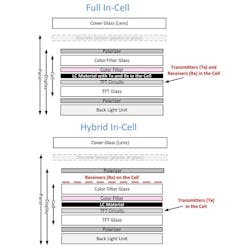
“In-cell” integration, where the sensors use existing display layers to construct the touch-sensor matrix, typically leverages the common electrode (or VCOM layer) as the touch-sensor matrix and the metal layers as interconnects to the matrix. For today’s in-plane switching (IPS) panels, these layers all exist on the TFT glass.
One other type of in-cell integration involves a hybrid design—the transmitting layer of the touch sensor is in-cell on the TFT glass while the receiving layer is on-cell on the color-filter glass. This is referred to as a “hybrid in-cell” design. To avoid confusion, the term “full in-cell” is used to indicate that the transmitting and receiving touch sensor layers are both within the cell. Figure 2 shows both types of in-cell designs.
Integrating the Touch Controller and Display Driver ICs
Historically, separate suppliers provide the ICs that control the touch and display functions. While integrating these separate ICs is possible with discrete panel stack-ups and on-cell displays, the benefits are limited and the effort becomes more complicated when dealing with multiple suppliers. In contrast, with in-cell integration, integrating the touch controller and the display driver into a single IC is both easier and substantially more beneficial.
The display functions in existing smartphones and tablets are likely controlled by a single display driver IC (DDIC), while the touch functions are probably controlled by a separate touch controller IC. In designs that use an on-cell display, the DDIC is always located on the TFT glass itself, referred to as chip-on-glass (COG), and the touch controller IC is usually located on a flexible printed circuit (FPC or flex), referred to as chip-on-flex (COF). In such designs, there are usually two FPCs from the host to the panel—one for the DDIC on the TFT glass, and the other for the touch controller.
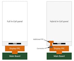
Smartphones and tablets designed with a full in-cell display require only a single FPC to interface with both the display and the touch sensor (Fig. 3). Having a single FPC makes a compelling case for integrating the touch controller and the display driver into a single IC, otherwise known as touch and display driver integration (TDDI). Because the IC itself has a CPU (for touch signal processing) and is mounted on the TFT glass, the integrated solution is sometimes referred to as a “smart display” that’s powered by TDDI.Note that TDDI can also be used for hybrid in-cell implementations. In this configuration, a second FPC is normally used to route the receiver pins (from the TDDI chip on the TFT glass) to the receiver electrodes on top of the color-filter glass (Fig. 3, again). This second FPC only contains the routing signals and doesn’t contain any active components.
The architectural design and implementation of TDDI solutions isn’t trivial. For advanced display noise management and improved capacitive-sensing performance, the latest designs now coordinate and synchronize the touch-sensing and display-update functions. The resulting design overcomes the limitations associated with discrete panel stack-ups and on-cell displays, where touch and display functions typically operate independently from one another.
Advantages of Display Integration Solutions
Some significant advantages can be derived from integrating the touch and display functions in both in-cell displays and the ICs. These advantages can be divided into two categories: those that benefit engineering, manufacturing, and support activities; and those that enhance the design of the smartphone or tablet.
Engineering, Manufacturing, and Support Advantages
Integrating touch and display functions in both the display stack-up and the IC simplifies the design effort, helping accelerate the time-to-market for new devices, which can give device manufacturers a distinct competitive advantage in rapidly evolving markets.
Manufacturing costs are minimized based on a combination of fewer components and a more efficient supply chain. There is one less FPC with full in-cell integration, and one less IC. The display panels ship from the LCD manufacturer with fully integrated touch capabilities, virtually eliminating yield loss from a separate sensor lamination process. Fewer components and suppliers mean fewer assembly steps and problems, and the devices require less work-in-process manufacturing time.
Engineering, manufacturing, and especially ongoing support all benefit from the streamlined supply chain that affords “one-stop-shopping,” with a single supplier being responsible for the entire touchscreen display-panel subassembly—edge-to-edge and top-to-bottom. Having a single supplier fully responsible for both the touch and display functions also streamlines troubleshooting efforts.
Device Design Advantages
The elegance and simplicity of integrating both the touch and display functions in both the display glass and the IC results in a sleeker, more functional device. With full in-cell displays, the panel is thinner compared to discrete designs. The display also has narrower borders because external routing isn’t needed on the sides or top of the display panel. Thinner panels result in thinner form factors or provide more space for other features, such as additional memory or battery capacity, while the narrower borders support the narrow bezels needed to produce full-size, edge-to-edge displays.
The combination of in-cell and TDDI also improves performance, because the display is more responsive to touch control, owing to the ability to isolate and synchronize the display update and touch-sensing functions. In addition, synchronizing the touch and display functions virtually eliminates electrical display noise from interfering with touch sensing, which can cause operational problems when not properly mitigated. And with no separate touch sensor layer to attenuate light, in-cell displays are about 10% brighter or, alternatively, can provide the same brightness with less backlight, resulting in longer battery life (Fig. 4).
Finally, integrating the touch and display functions simplifies the device’s design and manufacturability, so it also improves the device’s overall reliability. That’s because multiple functional layers needn’t be laminated, which could otherwise cause a malfunction or failure. In contrast, in a laminated discrete panel stack-up where the design itself might be causing a problem, the need to involve multiple suppliers complicates the effort to resolve any issues in a timely manner.
Conclusion
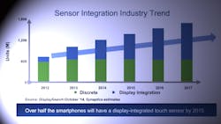
Touchscreens have become the norm in smartphones and tablets, and user demand for simplified navigation has made touchscreens nearly ubiquitous in laptops and all-in-one desktop PCs. Although many different technologies are now available for incorporating touch and display functions into touchscreens, the use of an in-cell display with TDDI is rapidly becoming the preferred choice for new devices in the mainstream mobile market.
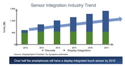
The reason for its rapidly increasing popularity is the ability to solve numerous problems caused by previous design and manufacturing methods for panel stack-ups (Fig. 5). Indeed, implementing touch and display functions in an autonomous and asynchronous manner has resulted in more complicated designs, increased costs, and less dependable operation. The full integration and synchronization of touch and display functions solves these problems and affords some other advantages that result in thinner and smarter devices, and, ultimately, more satisfied users.
This file type includes high resolution graphics and schematics when applicable.
About the Author
Kevin Barber
Senior Vice President and General Manager, Smart Display Division
Kevin Barber, Senior Vice President and General Manager of the Smart Display Division (SDD) for Synaptics since January 2011, has extensive domain expertise in the mobile communications industry. Prior to joining Synaptics, Mr. Barber was CEO of ACCO Semiconductor since 2008, and from 2007 to 2008, he served as a principal consultant at PRTM. He was Senior Vice President and General Manager of the Mobile Solutions business at Skyworks Solutions from 2003 to 2006, where he was responsible for delivering innovative RF products to the mobile industry. And he was Senior Vice President of Operations at Skyworks Solutions from 2002 to 2003 and Conexant Systems from 2001 to 2002. Previously, he held various senior operations positions at Conexant Systems and Rockwell Semiconductor. Mr. Barber holds a BSEE from San Diego State University and an MBA from Pepperdine University.
Comment About the Article
To join the conversation, and become an exclusive member of Electronic Design, create an account today!

Leaders relevant to this article: