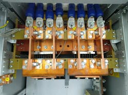
Why Bus Bars Excel At High-Performance Switching Apps
Regardless of a bus bar’s size or complexity, its fundamental purpose, like a wire or cable, is to connect two or more points of a circuit. Beyond this basic purpose, bus bars offer many other advantages over conventional cables. One particular advantage is this: a bus bar assembly can be manufactured so that it minimizes stray circuit inductance while making all required component connections. This is a useful feature for a number of applications, but is becoming a necessity for high-performance switching applications that use modern semiconductors.
Today’s semiconductor designers are continually improving their technology. Devices like MOSFETs, IGBTs and diodes have evolved considerably and are performing at levels one could only imagine 10 to 15 years ago. They have higher voltage ratings, lower conduction losses and faster switching speeds. This surely deserves applause, but without bus bars, the benefits of these advancements, specifically increased switching speed, could not be applied successfully.
Read More About Busbars
In a typical switching application such as a motor drive or converter, energy stored in a circuit’s “stray” inductance will be realized in the form of an overshooting voltage spike added to the DC bus voltage and felt across the IGBT at the time of turn-off. This overshoot voltage is proportional to the rate of change of current (di/dt) and the amount of stray inductance (L) in the circuit, supporting the formula V=L*di/dt. For example: In a circuit with a stray inductance of 100 nH, turning off an IGBT having a 50 ns fall time from 125 A (typical for modern 600 V IGBTs and equaling a di/dt of roughly 2000 A/µs) will result in an overshoot of the bus voltage by about 200 V (200 V = 100 nH * 2000 A/µs). If we assume a 450 V bus voltage, the additional 200 V overshoot experienced at turn-off makes the total voltage that needs to be supported by the IGBT approach 650 V. If a 600 V IGBT was planned for the application--typical for 450 V applications--this level of circuit reactance would spell disaster and most likely cause catastrophic damage to the IGBT.
As options, the circuit designer could increase the IGBT gate resistance (RG) and reduce the turn-off di/dt. This would reduce the overshoot voltage but also increase the turn-off loss and not take full advantage of the new semiconductor technology. The designer might also select a higher voltage IGBT, but higher voltage IGBTs have greater on-state voltage (VCE(SAT)) and, thus, increased conduction loss. Ironically, higher voltage IGBTs also have slower switching speeds than their lower voltage siblings; therefore, the overshoot voltage will likely be reduced to some degree. But the slower switching speed will result in an increased turn-off loss (EOFF), compromising circuit efficiency once again.
It should also be mentioned that a diode in the same circuit will experience a similar voltage spike when it is reverse biased as a result of turning on an IGBT elsewhere in the circuit. Again, the voltage rating will be exceeded and, assuming survival, the resulting reverse recovery loss will increase due to the spike voltage. If the IGBT turn-on is slowed or a higher voltage diode is selected, the designer will be faced with similar efficiency trade-offs as those explained for the IGBT.
Of course, safety margins must be designed into every circuit; therefore, designers should select devices that have voltage ratings appropriately greater than the bus voltage. For the sake of efficiency, however, and to minimize cooling requirements, one would prefer to use an IGBT having the lowest voltage rating that safety margins and cost will allow, presumably also having the lowest VCE(SAT) and fastest switching speeds. That said, the circuit designer must minimize stray inductance to fully capitalize on the semiconductor’s performance potential.
Stray Circuit Inductance and Multi-layer Busbars
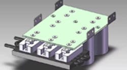
An effective way to minimize stray circuit inductance is to use a laminated multi-layer bus bar (Fig. 1). In this arrangement, the capacitors and IGBT modules are intimately connected to the conductors of the bus bar. These are typically made of copper and plated with Sn, Ni or other metal to slow oxidation and improve connection integrity. Component terminal offsets are compensated for with bushings or formed areas of the bus bar conductors themselves. The formed and plated conductors are then laminated together, separated by a thin layer or multiple layers of material having a high dielectric strength such as Mylar or Nomex.
If the conductors are properly shaped/routed so that current flows equally and in the opposite direction through each, their opposing magnetic fields will effectively cancel each other, resulting in little added circuit inductance. The closer the conductors are together, the more this effect is realized; therefore, the dielectric material selected should be as thin as possible but have a dielectric strength appropriately in excess of the application voltage. The majority of the remaining circuit inductance is typically due to the leads and internal lead connection of the bus capacitors. That said, depending on the capacitors selected, using a bus bar alone may or may not result in a sufficiently low enough total circuit inductance. If required, the circuit designer may add additional ultra-low-inductance bypass capacitors in parallel with the primary bus capacitors and in close vicinity of or directly across the IGBT terminals (C1-E2), yet again lowering circuit inductance. These capacitors are commonly referred to as snubber capacitors, but are more accurately being used in a bypass role. It’s worth mentioning that some inductance can also be attributed to the IGBT packaging itself; however, semiconductor designers are painfully aware of the detrimental effects of stray inductance and go to great lengths to reduce it as much as possible in their packaging. Many modern semiconductor packages employ miniature versions of multi-layer bus bars internally.
Typically not viewed as cutting-edge technology, the bus bar’s contribution to improved circuit performance often goes unnoticed. Its capability goes well beyond that of cables or wires. With a multi-layer bus bar’s proper design and use, the circuit designer can fully realize the performance benefits of today’s modern power semiconductors. Even high-voltage semiconductors (rated above 3 kV) have evolved to the point where low-inductance circuit construction is an absolute necessity. Laminated multi-layer bus bars are a time-proven way to achieve this and offer numerous advantages over other interconnect choices. Bus bars should be thought of as an essential part of every high-performance switching application and are truly an enabling technology.
About the Author

Ken Brandmier
Director of New Product Development
Ken is the Director of New Product Development at Custom Electronics, Inc.


