Opportunities and Challenges for Next-Gen Semiconductor Integration
>> Electronic Design Resources
.. >> Library: Article Series
.. .. >> Series: Path to Systems
Download this article in PDF format.
In the 70 years since the transistor was invented1 and 60 years since the integrated circuit (IC) was invented,2 we have taken the computer out of large rooms and put them into our pockets. It’s been an amazing time where we have been able to impact every aspect of society with the innovations enabled by these two moments in history. Now we’re in the process of taking the computer out of our pockets and putting it into our clothing, into our bodies, and into our imaginations.
At the same time, we have completely removed the need for wires when communicating with other people throughout the world. Instead of having to fly halfway around the world for a face-to-face conversation, we can do that instantaneously with the push of a button. Now instead of suffering from “jetlag”, we instead suffer from “netlag.” It’s amazing now to find ourselves on the threshold of computers talking and listening to us in the same ways we communicate with other people. Computers, of course, now talk to each other without human intervention. One can only guess what will be next.
These advances have created several challenges (or should we say opportunities) for electronic designs and therefore the semiconductor industry:
- The focus of electronic design has moved from the component to the system.
- The demand for performance has outstripped our capacity and capability.
- The demand for ultra-low power (e.g., long battery life) has become the new performance metric.
- There’s a continuous demand for faster product introduction cycles.
- The innovation enabled by using technology no longer requires us to understand the technology we’re using.
In this article, we’ll discuss the opportunities that are ahead for the semiconductor industry and how they will drive the next round of innovation. Then we’ll propose an idea on how to enable the next round of innovation. Finally, we’ll make some concluding remarks as to our view of that exciting future.
Opportunity
One of the interesting evolutions that has occurred in the semiconductor industry is the move in focus from the component to the system. That is, instead of just creating components, which can then be used to create systems, the focus is to now create a system design and then determine the optimal set of components needed to implement that system. This may seem to be a subtle change, but is a valuable insight to help us continue the integration path Dr. Gordon Moore envisioned in 1965.3
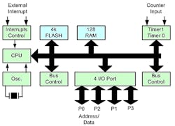
1. The first microcontroller was developed in 1971 by Texas Instruments, which had a block diagram similar to the one shown.
If we look back at early microprocessor and microcontroller devices, they had very little integrated memory and typically had no industry-standard peripherals (Fig. 1). Compare that to contemporary microprocessors (Fig. 2), which are complete systems with all (yes using the word “all” is a bit of an overstatement) of the memory and peripherals needed for a complete computer system.4
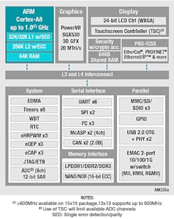
2. The block diagram represents Texas Instruments’ AM335x ARM Cortex-A8 based microprocessor system-on-chip.
However, the pace of integration and increased performance in processor systems haven’t exactly kept up with the demand for performance from the software and embedded-systems designers as they grow hungrier for more every year. The performance demands at the beginning of the microcomputer era to create new audio or video products were well within the state of the art of semiconductor technology.
But we’re now seeing opportunities in fields such as artificial intelligence (AI), machine learning, image understanding, and cloud computing stretching the limits of contemporary performance. Not only are these applications demanding exponentially more performance, they also want better integration of heterogeneous components such as FPGAs, GPUs, hardware accelerators, and processors for targeted applications. These demands are driving the performance requirements well beyond Moore’s law.5
At the same time, we’re seeing computer systems shrinking, with the end goal being the concept of “smart dust”.6 To make this possible, the focus changes from driving performance to reducing power dissipation so as to, in the end, power these devices using as little energy as body heat.7
During the past 10 years, with the advent of smart devices, the electronics consumer industry has been in a constant state of competition that has driven semiconductor innovation to an unprecedented level. With the design services market segment forecasted to grow with a 7.24% CAGR between 2018 to 2023,8 there has been a consistent demand for ways consumer electronics companies could reduce/eliminate the effort they have to invest to introduce new products by abstracting the menial tasks of system design.
Finally, the most interesting aspect of the opportunities ahead is the ability to use technology without the need to deeply understand it. Platforms like Arduino,9 Raspberry Pi,10 and BeagleBone11 have made it possible for creative non-engineers to take advantage of the technology to innovate in their areas of passion. As this non-technical creative community begins to create new requirements for semiconductor devices, it’s important to make sure those requirements are met in a meaningful way. The goal is to eliminate the increasingly higher barriers of entry that surround electronic design and manufacturing.
The System-in-Package Solution
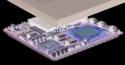
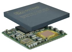
The key to successfully create any solution is to first find the need to be realized and then find the technology that makes it possible. For the semiconductor industry, this solution needs to enable system designers and product developers to simplify product design while offering them what they need in terms of performance and features, essentially addressing each of the opportunities described earlier. We argue that the solution lies in system-in-package (SiP) (Fig. 3).
3. System-in-package integrates a diverse set of semiconductor components and passives into one package, miniaturizing the hardware while also simplifying design and manufacturing.
There are fundamental requirements that the proposed SiP solution should satisfy, without which its usefulness is limited. The requirements are:
- The integration of diverse active semiconductor components and passive components into one system where the active components could be microprocessors, memories, specialized processing devices, analog circuits, power management, and sensors.
- The miniaturization of the resulting implementation and system footprint.
- Scalability allowing for low-volume opportunities to high-volume opportunities without a cost burden to either end of the scale.
- The ability to provide system-level hardware sub-modules of often-used subsystems. You might call this sub-system-in-package (SSiP).
- Quick, low-cost, prototyping and testing alternatives through flexibilities in design and interconnection methodologies.
This is where the concept of “what is good in the world of semiconductors” complements the concept of “what is good in the world of systems.” For example, the concept of fan-out wafer-level packaging (FO-WLP)12,13,14 has been developed to allow the creation of semiconductor devices that shrink feature size of the IC beyond the physical constraints of a system design. The result is taking semiconductor die that are too small to use as a system-level component and putting them in larger packages, made up of low-cost materials, which are large enough to be used in system designs. The size of these larger packaged components enables them to be used on printed circuit boards (PCBs) to create custom systems.
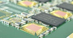
This currently existing technology is one proposed solution that addresses some of the opportunities that we discussed. Though it’s a step in the right direction, it doesn’t satisfy all of the requirements of a system component. It partially addresses the complexity of design and manufacturing issues, but doesn’t allow for miniaturization or higher level of integration, both of which can be addressed in a SiP solution. As we discuss more about the proposed SiP solution in our series, we will delve into how each of these requirements can be satisfied (Fig. 4).
4. SiP technology can solve a lot of existing electronics design and manufacturing issues, allowing for faster and easier development of electronics.
Finally, it’s important to characterize the target areas and markets for SiP technology, as the semiconductor industry is also vastly diverse in its requirements. These requirements may sometimes include specialized functionalities and custom hardware that might not fit within the SiP framework. But, advances and improvements to the existing SiP architecture can help address most use cases. The goal of this article series will be to make a compelling value proposition for system-in-package technology while addressing how it beats the challenges presented by the opportunities introduced in this article.
Looking Ahead
Significant levels of semiconductor integration have already been achieved, and consumers are already benefiting from this through smaller and better performing smartphones and other electronic devices. As we develop new ways of 2.5D and 3D integration that reduce cost and increase manufacturability, it’s important to look at the bigger picture in terms of needs and technologies and to connect them in a meaningful way.
The bigger picture for electronic system design would be to have a design flow that’s both systems-centric (SiP and PCB) and component-centric (SoC). The system-centric portion of the design flow requires the ability to integrate various semiconductor devices that are each manufactured with its own optimized process, along with hundreds of passive devices.
Finally, the overall design flow from IC creation to system creation needs to economically scale up or down (both volume and cost) without burdening either end of the design flow. We will see in future articles in the series how system-in-package technology provides a perfect sweet spot to solve many design and manufacturing problems while addressing new opportunities and requirements.
References:
- Michael Riordan, “The Lost History of the Transistor”, in IEEE Spectrum, 2004
- Jack S. Kilby, “Miniaturized Electronic Circuits”, US Patent 3,138,743, June 23, 1964
- Gordon E. Moore, Cramming more components onto integrated circuits, Electronics, April 19, 1965.
- A. A. Pachghare, G. K. Andurkar, A. M. Kulkarni, “A review on Microprocessor and Microprocessor Specification”, in International Journal of Science, Engineering and Technology Research (IJSETR) Volume 2, Issue 2, February 2013
- J. A. Carballo, W. T. J. Chan, P. A. Gargini, A. B. Kahng and S. Nath, "ITRS 2.0: Toward a re-framing of the Semiconductor Technology Roadmap," 2014 IEEE 32nd International Conference on Computer Design (ICCD), Seoul, 2014, pp. 139-146.
- B. Warneke, M. Last, B. Liebowitz and K. S. J. Pister, "Smart Dust: communicating with a cubic-millimeter computer," in Computer, vol. 34, no. 1, pp. 44-51, Jan 2001.
- Body heat: M. Highland eet al., "Wearable Thermoelectric Generators for Human Body Heat Harvesting," Appl. Energy 182, 518, 2016
- Global Electronic Contract Design Engineering Market - Segmented by Type of Activity, Application, and Geography - Growth, Trends, and Forecast (2018 - 2023)
- https://www.arduino.cc/
- https://www.raspberrypi.org/
- http://beagleboard.org/bone
- Yonggang Jin, et al, Next Generation eWLB (embedded Wafer Level BGA) Packaging, 2010 EPTC.
- J. Campos, et al. System in Package Solutions using Fan-Out Wafer Level Packaging Technology, June 27, 2013, Semi.
- Ron Huemoeller, Silicon wafer integrated fan-out technology, April 2015, Chipscale Review.

About the Author
Neeraj Dantu
Applications and Systems Engineer
Neeraj Dantu is an Applications and Systems Engineer at Octavo Systems. As a recent graduate, Neeraj is excited to be a part of Octavo’s highly experienced team. He also looks forward to help Octavo change the face of electronic design and manufacturing. With diverse research experience in hardware design, machine learning, computer vision, and signal processing, Neeraj brings a fresh perspective to the team. Neeraj earned his B.Tech (Bachelor of Technology) in Electronics and Communications Engineering from The LNM Institute of Information Technology, India, and a Masters in Electrical Engineering from Rice University.
Gene Frantz
Chief Technology Officer
Masood Murtuza
Co-founder and Manager of Package Engineering
Masood Murtuza is the Manager of Package Engineering and a founder of Octavo Systems. Prior to joining Octavo, Masood was a Fellow at Texas Instruments, where he held various leadership roles in the Packaging and Assembly Process Engineering teams. During his tenure at TI, he introduced a number of new semiconductor packaging technologies. He also helped advance innovation in technology development across the company by establishing new methodologies in package and assembly development process. Masood holds 25 patents and has authored or co-authored over 15 papers. He received his BTech in Mechanical Engineering from the Indian Institute of Technology, Madras, India, and an MSc in Naval Architecture from University College, University of London.
Gene Frantz
Chief Technology Officer
Gene Frantz is one of the founders and the visionary behind Octavo Systems. He currently serves as Chief Technology Officer. He is also a Professor in the Practice at Rice University in the Electrical and Computer Engineering Department. Previously, Gene was the Principal Technology Fellow at Texas Instruments, where he built a career finding new opportunities and building new businesses to leverage TI’s DSP technology. Through this work he became highly regarded in the industry as a leader in DSP technology. Gene holds 48 patents, has written over 100 papers/articles, and presents at conferences around the globe. He has a BSEE from the University of Central Florida, a MSEE from Southern Methodist University, and a MBA from Texas Tech University. He is also a Fellow of the IEEE.
Comment About the Article
To join the conversation, and become an exclusive member of Electronic Design, create an account today!

Leaders relevant to this article: