Why a SiP?
>> Electronic Design Resources
.. >> Library: Article Series
.. .. >> Series: Path to Systems
Integration has been the driving function of the semiconductor industry since the transistor was invented. An underlying assumption is that putting more transistors on a piece of silicon was the answer—now, “what was your question?” Many years ago, we used terms like SSI, MSI, and LSI (small-scale integration, medium-scale integration and large-scale integration, respectively). These terms represented a progression of technology and processes for transistor integration.
This progression did not, however, describe the functional integration that came as a result. Consequently, descriptions such as ASIC and SoC (application-specific integrated circuit and system-on-chip) were termed. All of these terms helped to keep in perspective the drive toward more system integration. For example, Figure 1 shows the difference in functionalities of two DSP SoCs from Texas Instruments (TI) about 10 years apart from each other.
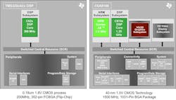
1. Comparing the integration of two processors, 10 years apart.
Along with the increased performance at a much smaller technology node, the C6A8168 processor integrates custom cores for graphics processing, video display, and a Cortex A8 ARM core. Along with these cores, the newer processor also integrates several subsystems for connectivity, timing, data storage, and peripherals. The comparison shows how far the industry has come.
As we move forward in this area with integration both at a transistor level and a functional level, new advances in package and circuit board technology have given rise to terms like MCM, SOM, and SiP (multichip module, system-on-module, and system-in-package).
The topic of this paper is this latest descriptor of integration. We will use the term system-in-package (SiP), as it best describes what it is—the next revolution in circuit integration. Let’s start with an “under the hood” view of a SiP device.
Under the Hood
The general concept behind the development of a SiP is the unspoken result of pursuing Moore’s Law. That is, to keep driving integration, we needed to focus the silicon process development on each of the different kinds of circuits. For example, as the microprocessor needed a different process than that of a memory device, analog circuit, a power-management device, or a sensor device, the obvious answer was to integrate at the system level. This can be termed as the origin for SiP technology.
Despite the relative newness of the term, SiPs have been around for a long time in one form or another. Discretionary wiring1, MCMs, and Hybrid Integrated Circuits (HIC)2 have been done in the 1970s. Early adaption of the current form of SiP technology took place in the late ’90s with Intel’s Pentium Pro3 integrating processor and cache on separate dies. In contrast to the early days, SiP has transformed into a niche solution with applications in wireless communication and sensors.
The SiP is a semiconductor device in which systems are integrated. Figure 2 shows an example of a SiP, the OSD335x-SM. The components of a SiP include die; in this example, it’s wire-bonded to a substrate. There can be more than one die oftentimes that’s heterogeneous, like power-management ICs, analog PHYs, and memories. The SiP can also integrate packaged parts and other SiP modules. Furthermore, the integration techniques also might vary for example stacked die, flip-chip, through silicon via (TSV), or 3D SiC (3D stacked IC).
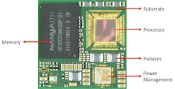
2. Shown is Octavo Systems’ OSD335x-SM, revealing the components of a SiP.
Why Use a SiP?
The last few years have not been great for Moore’s Law. Moving to the next processing node now requires billions of dollars in investment. As a result, the industry is looking at optimizing processes and producing efficient semiconductor products while searching for better paths of integration.
The industry is also facing long design cycles. Embedded systems of present day have complex functionalities implemented on high-speed data lanes and protocol specific PHYs. A lot of high-speed interfaces like Ethernet use analog signaling. Many products now also have analog signal conditioning and processing blocks that don’t fit into the SoC. MEMs sensors are a good example. Memory is another non-logic component that’s now being integrated into most IoT/embedded devices. All of this makes for complex embedded systems, but with striking commonalities.
Even as keeping up with Moore’s Law has been difficult for logic, process scaling has been harder on analog and mixed-signal design. As a result, we no longer have just one IC manufacturing process. As seen in Figure 3, we have created processes to be optimized for specific needs. There’s an optimized process for high-performance microprocessors, memories, high-performance audio power management, and RF circuits.
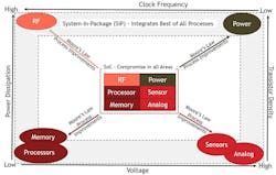
3. Moore’s Law has caused semiconductor processes to progress in multiple directions.
Due to the components with high-speed interfaces that need to be discretely integrated, the end product is often complex, driving design and manufacturing costs higher. Along with adding design complexity and time to market, this sets fundamental limitations on the new and innovative products with a high barrier of entry for new companies in systems design.
SiP technology addresses all of these problems. Some of the advantages are described below:
Simplification: System designers can integrate SiP components as abstract building blocks that allow them to design faster, enabling a much smaller design cycle. Double-data-rate (DDR) interface design is a prime example for this advantage. DDR layout along with power design and distribution are among the common places that demands a re-spin/redesign. The complexity in the current design environment is resulting in design cycles of 12-24 months. Depending on what a SiP integrates, the design cycle can be cut in half, often with no need for lots of hardware design experience in the team. Moreover, the system-based approach to integration allows for simplified mill of materials (BOM), eliminating debugging for trivial but important interfaces like DDR. This results in getting to a finished product much faster than otherwise.
Manufacturability and yield: Though manufacturability is a constantly evolving concept when it comes to the semiconductor industry, the less complex the design, i.e. lower-speed interfaces, higher tolerances, and relaxed design rules, the higher the manufacturability of the product. This is an area where SiP expertise comes in very handy. Akin to cooking with the right recipe, given the right approach to SiP design, with substrate selection, mold compound selection, and thermo-mechanical modeling, yield and manufacturability can be extremely positive.
Miniaturization: Another highly valued aspect of semiconductors, especially in this smart gadget IoT era, is minimizing the size of the system. On an average system where only 10% of the components are ICs,4 miniaturization is a difficult process and sometimes isn’t possible without compromise or a higher-cost system. SiP design rules allow for not only much tighter die integration, but also closer passive integration. This reduces the overall size of the system by as much as 65%.5 So, in a lot of ways, SiP can be viewed as complementary to Moore’s Law with a system-level approach to integration.
Cost reduction: Miniaturization is often associated with increased cost. That actually might be not true in the case of system-in-package due to the economics of scale in the semiconductor industry. That’s because the cost of manufacturing with a number of integrated components in high volumes reduces the cost for all customers. Cost reduction doesn’t stop there. Assembly cost, discrete BOM overhead, and PCB design cost can see big reductions depending on the system. An analysis for the OSD335x SiPs shows up to 20% cost savings.
Reliability: Compared to a PCB system using discrete components (ICs, passive devices), a SiP is equal or better in terms of failure probability. SiPs use the same qualified set of silicon and passive devices as their packaged component version do, thus the intrinsic reliability of these individual components will be the same. The potential improvement comes by way of solder joint reliability. In the case of molded SIPs, such as OSD3358-BSM, the solder joints of constituent packaged IC devices and passive devices are fully encapsulated in a molding compound. Molding compound protects the solder joints from stresses.
The most common loads that cause failure in soldered components are due to board flexure and bending, shock and vibration, and temperature cycles. In each of these cases, stress is significantly reduced because of the protective molding compound surrounding the components. In addition, SIPs are put through the same intensive qualification tests as semiconductor components; these tests are generally more stringent than commonly used PCB qualification tests. Figure 4 shows the results of a typical qualification test applied to OSD3358-BSM.
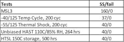
4. The results of a typical qualification test applied to OSD3358-BSM.
Next-generation requirements: Continuing the pursuit of monolithic SoC development poses roadblocks on multiple fronts. Design verification and manufacturability become harder as the size of the die increases simply because of the greater chance of impurity/manufacturing faults on a larger die.
Another key issue is intellectual property and the legal issues that arise with design reuse. As new advances such as more efficient communication protocols and modulation techniques are invented, trying to design monolithic dies that keep up is neither economic nor fast. In this context, SiP is a great alternative. On the other side of the spectrum, SiP also eliminates/significantly reduces limitations of current PCB manufacturing technology. SiP reduces the system form factor, significantly increases the chip-to-chip bandwidth, and reduces the power consumption of the system via short and thin electrical traces.
But What Are the Issues?
But disadvantages also need to be addressed: lack of flexibility; inability to customize, and the need to be high volume to be viable in the IC manufacturing process.
Lack of Flexibility
Since SiPs are systems rather than components, they are by their very nature application-dependent and tend to be more application-specific than SoCs. SoCs are designed to be components used in many systems and therefore tend to not be customer-specific, but designed as standard components. Thus, the economies of scale found in high-volume SoCs are lost in the world of SiPs.
Inability to Customize
Systems built with discrete components offer a great deal of flexibility in their design and development; small changes in design are often accommodated without extensive redesign. Such changes aren’t practical in SiPs because major components like the substrate or interconnecting systems require major revisions involving a redesign of the substrate. A redesign not only will add cost to the project, but also create a schedule delay of several months. Ideally, one would like to have a SiP with the flexibility of a discrete component system, yet still have the economies of scale of an SoC.
Need for High Volume
The semiconductor industry has been successful due to its drive to lower the cost of manufacturing. A key component of this drive is high-volume manufacturing methods. That creates a significant issue to a system design which only needs thousands per month rather than millions per month. It’s obvious that the need for high volume is key to the success of any IC technology, including SiP technology. The question is how to provide low-volume system components while not altering the high-volume manufacturing flow.
Conclusion
In the previous article of this series, we described the opportunities and challenges ahead for the semiconductor industry. The focus has shifted from component view to system view of design, and the industry demands higher performance with a lower complexity and higher manufacturability. However, the most important aspects of the innovation that has always driven electronics are miniaturization and low barrier for entry. SiP makes both of these goals possible. With the next generation of requirements such as terabit networking, 5G wireless, and 8K video posing tough challenges, having the advantages that SiP brings to the table becomes very important for success. SiP essentially extends the life of Moore’s Law. By how much? That’s yet to be determined.
- Series: Path to Systems
- Prior article in this Series ... Opportunities and Challenges for Next-Gen Semiconductor Integration
- Next article in this Series ... SiP—Leveraging Mass Production on a Small Scale
References:
- http://www.computerhistory.org/siliconengine/application-specific-integrated-circuits-employ-computer-aided-design/
- https://patents.google.com/patent/US5559374A/en
- http://www.dexsilicium.com/Intel_Pentium Pro.pdf
- https://electroiq.com/2006/07/soc-vs-mcm-vs-sip-vs-sop/
- https://octavosystems.com/2017/08/30/smaller-cheaper-pcbs/

About the Author
Neeraj Dantu
Applications and Systems Engineer
Neeraj Dantu is an Applications and Systems Engineer at Octavo Systems. As a recent graduate, Neeraj is excited to be a part of Octavo’s highly experienced team. He also looks forward to help Octavo change the face of electronic design and manufacturing. With diverse research experience in hardware design, machine learning, computer vision, and signal processing, Neeraj brings a fresh perspective to the team. Neeraj earned his B.Tech (Bachelor of Technology) in Electronics and Communications Engineering from The LNM Institute of Information Technology, India, and a Masters in Electrical Engineering from Rice University.
Gene Frantz
Chief Technology Officer
Masood Murtuza
Co-founder and Manager of Package Engineering
Masood Murtuza is the Manager of Package Engineering and a founder of Octavo Systems. Prior to joining Octavo, Masood was a Fellow at Texas Instruments, where he held various leadership roles in the Packaging and Assembly Process Engineering teams. During his tenure at TI, he introduced a number of new semiconductor packaging technologies. He also helped advance innovation in technology development across the company by establishing new methodologies in package and assembly development process. Masood holds 25 patents and has authored or co-authored over 15 papers. He received his BTech in Mechanical Engineering from the Indian Institute of Technology, Madras, India, and an MSc in Naval Architecture from University College, University of London.
Gene Frantz
Chief Technology Officer
Gene Frantz is one of the founders and the visionary behind Octavo Systems. He currently serves as Chief Technology Officer. He is also a Professor in the Practice at Rice University in the Electrical and Computer Engineering Department. Previously, Gene was the Principal Technology Fellow at Texas Instruments, where he built a career finding new opportunities and building new businesses to leverage TI’s DSP technology. Through this work he became highly regarded in the industry as a leader in DSP technology. Gene holds 48 patents, has written over 100 papers/articles, and presents at conferences around the globe. He has a BSEE from the University of Central Florida, a MSEE from Southern Methodist University, and a MBA from Texas Tech University. He is also a Fellow of the IEEE.
Comment About the Article
To join the conversation, and become an exclusive member of Electronic Design, create an account today!

Leaders relevant to this article: